Nature ( IF 50.5 ) Pub Date : 2022-11-30 , DOI: 10.1038/s41586-022-05329-1 Johann Riemensberger 1, 2 , Nikolai Kuznetsov 1, 2 , Junqiu Liu 1 , Jijun He 1 , Rui Ning Wang 1, 2 , Tobias J Kippenberg 1, 2
|
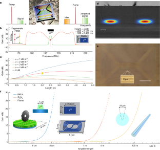
The ability to amplify optical signals is of pivotal importance across science and technology typically using rare-earth-doped fibres or gain media based on III–V semiconductors. A different physical process to amplify optical signals is to use the Kerr nonlinearity of optical fibres through parametric interactions1,2. Pioneering work demonstrated continuous-wave net-gain travelling-wave parametric amplification in fibres3, enabling, for example, phase-sensitive (that is, noiseless) amplification4, link span increase5, signal regeneration and nonlinear phase noise mitigation6. Despite great progress7,8,9,10,11,12,13,14,15, all photonic integrated circuit-based demonstrations of net parametric gain have necessitated pulsed lasers, limiting their practical use. Until now, only bulk micromachined periodically poled lithium niobate (PPLN) waveguide chips have achieved continuous-wave gain16,17, yet their integration with silicon-wafer-based photonic circuits has not been shown. Here we demonstrate a photonic-integrated-circuit-based travelling-wave optical parametric amplifier with net signal gain in the continuous-wave regime. Using ultralow-loss, dispersion-engineered, metre-long, Si3N4 photonic integrated circuits18 on a silicon chip of dimensions 5 × 5 mm2, we achieve a continuous parametric gain of 12 dB that exceeds both the on-chip optical propagation loss and fibre–chip–fibre coupling losses in the telecommunication C band. Our work demonstrates the potential of photonic-integrated-circuit-based parametric amplifiers that have lithographically controlled gain spectrum, compact footprint, resilience to optical feedback and quantum-limited performance, and can operate in the wavelength ranges from visible to mid-infrared and outside conventional rare-earth amplification bands.
中文翻译:
光子集成连续行波参量放大器
放大光信号的能力对于通常使用稀土掺杂光纤或基于 III-V 族半导体的增益介质的科学技术至关重要。放大光信号的另一种物理过程是通过参数相互作用1,2使用光纤的克尔非线性。开创性的工作展示了光纤中的连续波净增益行波参量放大3,例如,能够实现相位敏感(即无噪声)放大4、链路跨度增加5、信号再生和非线性相位噪声抑制6。尽管取得了很大进步7,8,9,10,11,12,13,14,15, 所有基于光子集成电路的净参量增益演示都需要脉冲激光器,限制了它们的实际应用。到目前为止,只有块状微加工周期性极化铌酸锂 (PPLN) 波导芯片实现了连续波增益16,17,但它们与基于硅晶片的光子电路的集成尚未显示出来。在这里,我们展示了一种基于光子集成电路的行波光参量放大器,在连续波范围内具有净信号增益。在尺寸为 5 × 5 mm 2的硅芯片上使用超低损耗、色散设计、一米长的 Si 3 N 4光子集成电路18,我们实现了 12 dB 的连续参数增益,超过了电信 C 波段的片上光传播损耗和光纤-芯片-光纤耦合损耗。我们的工作展示了基于光子集成电路的参量放大器的潜力,这些放大器具有光刻控制的增益光谱、紧凑的占地面积、对光反馈的弹性和量子限制性能,并且可以在从可见光到中红外和室外的波长范围内工作常规稀土放大带。


 京公网安备 11010802027423号