当前位置:
X-MOL 学术
›
Nano Lett.
›
论文详情
Our official English website, www.x-mol.net, welcomes your
feedback! (Note: you will need to create a separate account there.)
Modulation Doping of Single-Layer Semiconductors for Improved Contact at Metal Interfaces
Nano Letters ( IF 9.6 ) Pub Date : 2022-11-28 , DOI: 10.1021/acs.nanolett.2c04011 Yeonchoo Cho 1, 2 , Gabriel R Schleder 3 , Daniel T Larson 2 , Elise Brutschea 4 , Kyung-Eun Byun 1 , Hongkun Park 2, 4 , Philip Kim 2 , Efthimios Kaxiras 2, 3
Nano Letters ( IF 9.6 ) Pub Date : 2022-11-28 , DOI: 10.1021/acs.nanolett.2c04011 Yeonchoo Cho 1, 2 , Gabriel R Schleder 3 , Daniel T Larson 2 , Elise Brutschea 4 , Kyung-Eun Byun 1 , Hongkun Park 2, 4 , Philip Kim 2 , Efthimios Kaxiras 2, 3
Affiliation
|
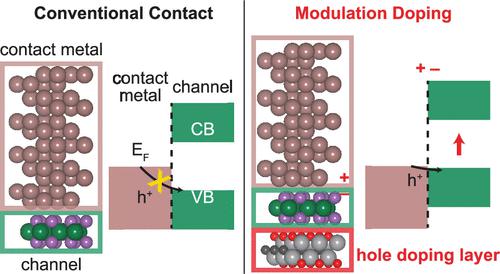
Single layers of two-dimensional (2D) materials hold the promise for further miniaturization of semiconductor electronic devices. However, the metal–semiconductor contact resistance limits device performance. To mitigate this problem, we propose modulation doping, specifically a doping layer placed on the opposite side of a metal–semiconductor interface. Using first-principles calculations to obtain the band alignment, we show that the Schottky barrier height and, consequently, the contact resistance at the metal–semiconductor interface can be reduced by modulation doping. We demonstrate the feasibility of this approach for a single-layer tungsten diselenide (WSe2) channel and 2D MXene modulation doping layers, interfaced with several different metal contacts. Our results indicate that the Fermi level of the metal can be shifted across the entire band gap. This approach can be straight-forwardly generalized for other 2D semiconductors and a wide variety of doping layers.
中文翻译:

单层半导体的调制掺杂以改善金属界面的接触
单层二维 (2D) 材料有望使半导体电子设备进一步小型化。然而,金属-半导体接触电阻限制了器件性能。为了缓解这个问题,我们提出了调制掺杂,特别是将掺杂层放置在金属-半导体界面的另一侧。使用第一性原理计算获得能带对齐,我们表明肖特基势垒高度以及金属-半导体界面处的接触电阻可以通过调制掺杂降低。我们证明了这种方法对于单层二硒化钨 (WSe 2) 通道和 2D MXene 调制掺杂层,与几个不同的金属触点连接。我们的结果表明,金属的费米能级可以在整个带隙内移动。这种方法可以直接推广到其他二维半导体和各种掺杂层。
更新日期:2022-11-28
中文翻译:
单层半导体的调制掺杂以改善金属界面的接触
单层二维 (2D) 材料有望使半导体电子设备进一步小型化。然而,金属-半导体接触电阻限制了器件性能。为了缓解这个问题,我们提出了调制掺杂,特别是将掺杂层放置在金属-半导体界面的另一侧。使用第一性原理计算获得能带对齐,我们表明肖特基势垒高度以及金属-半导体界面处的接触电阻可以通过调制掺杂降低。我们证明了这种方法对于单层二硒化钨 (WSe 2) 通道和 2D MXene 调制掺杂层,与几个不同的金属触点连接。我们的结果表明,金属的费米能级可以在整个带隙内移动。这种方法可以直接推广到其他二维半导体和各种掺杂层。


 京公网安备 11010802027423号