当前位置:
X-MOL 学术
›
ACS Photonics
›
论文详情
Our official English website, www.x-mol.net, welcomes your
feedback! (Note: you will need to create a separate account there.)
Capturing the Effects of Spatial Process Variations in Silicon Photonic Circuits
ACS Photonics ( IF 6.5 ) Pub Date : 2022-11-22 , DOI: 10.1021/acsphotonics.2c01194 Yufei Xing 1, 2 , Jiaxing Dong 1, 2 , Umar Khan 1, 2 , Wim Bogaerts 1, 2
ACS Photonics ( IF 6.5 ) Pub Date : 2022-11-22 , DOI: 10.1021/acsphotonics.2c01194 Yufei Xing 1, 2 , Jiaxing Dong 1, 2 , Umar Khan 1, 2 , Wim Bogaerts 1, 2
Affiliation
|
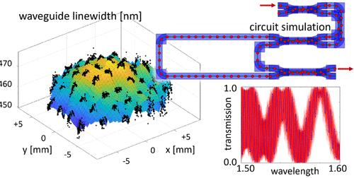
Silicon photonic devices are very sensitive to process variation, and it is important for circuit designers that they can predict the effect of this variability during the design phase, and optimize their design for both performance and yield. This requires an accurate predictive model of the spatial variations induced by the fabrication process. We present in this paper a method to extract a granular map of the line width and thickness variation on a silicon photonics wafer. We propose a hierarchical model to separate the layout-dependent and location-dependent systematic process variation from the random process variation on different spatial levels. We identify the relative contributions to width and thickness variations and use this to construct a synthetic model for virtual wafers that can be used to analyze the effect on circuit behavior and eventually predict the yield of photonic circuits after fabrication. We observe that the main contribution to waveguide width and thickness variations are systematic, and that die-scale systematic line width variation is correlated with local pattern density.
中文翻译:

捕获硅光子电路中空间过程变化的影响
硅光子器件对工艺变化非常敏感,对于电路设计人员来说,重要的是他们可以在设计阶段预测这种变化的影响,并优化他们的设计以提高性能和产量。这需要一个由制造过程引起的空间变化的准确预测模型。我们在本文中介绍了一种提取硅光子晶圆上线宽和厚度变化的粒度图的方法。我们提出了一个分层模型,将布局相关和位置相关的系统过程变化与不同空间水平上的随机过程变化分开。我们确定了对宽度和厚度变化的相对贡献,并使用它来构建虚拟晶圆的合成模型,该模型可用于分析对电路行为的影响,并最终预测制造后光子电路的产量。我们观察到波导宽度和厚度变化的主要贡献是系统性的,并且芯片级系统线宽变化与局部图案密度相关。
更新日期:2022-11-22
中文翻译:
捕获硅光子电路中空间过程变化的影响
硅光子器件对工艺变化非常敏感,对于电路设计人员来说,重要的是他们可以在设计阶段预测这种变化的影响,并优化他们的设计以提高性能和产量。这需要一个由制造过程引起的空间变化的准确预测模型。我们在本文中介绍了一种提取硅光子晶圆上线宽和厚度变化的粒度图的方法。我们提出了一个分层模型,将布局相关和位置相关的系统过程变化与不同空间水平上的随机过程变化分开。我们确定了对宽度和厚度变化的相对贡献,并使用它来构建虚拟晶圆的合成模型,该模型可用于分析对电路行为的影响,并最终预测制造后光子电路的产量。我们观察到波导宽度和厚度变化的主要贡献是系统性的,并且芯片级系统线宽变化与局部图案密度相关。


 京公网安备 11010802027423号