当前位置:
X-MOL 学术
›
Nano Lett.
›
论文详情
Our official English website, www.x-mol.net, welcomes your feedback! (Note: you will need to create a separate account there.)
Formation of In-Plane Semiconductor–Metal Contacts in 2D Platinum Telluride by Converting PtTe2 to Pt2Te2
Nano Letters ( IF 10.8 ) Pub Date : 2022-11-18 , DOI: 10.1021/acs.nanolett.2c03715 Kinga Lasek 1 , Jingfeng Li 1 , Mahdi Ghorbani-Asl 2 , Salma Khatun 1 , Onyedikachi Alanwoko 1 , Vimukthi Pathirage 1 , Arkady V Krasheninnikov 2, 3 , Matthias Batzill 1
Nano Letters ( IF 10.8 ) Pub Date : 2022-11-18 , DOI: 10.1021/acs.nanolett.2c03715 Kinga Lasek 1 , Jingfeng Li 1 , Mahdi Ghorbani-Asl 2 , Salma Khatun 1 , Onyedikachi Alanwoko 1 , Vimukthi Pathirage 1 , Arkady V Krasheninnikov 2, 3 , Matthias Batzill 1
Affiliation
|
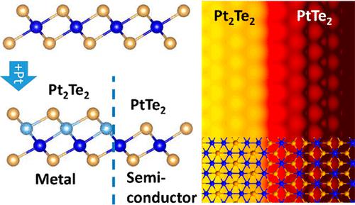
Monolayer PtTe2 is a narrow gap semiconductor while Pt2Te2 is a metal. Here we show that the former can be transformed into the latter by reaction with vapor-deposited Pt atoms. The transformation occurs by nucleating the Pt2Te2 phase within PtTe2 islands, so that a metal–semiconductor junction is formed. A flat band structure is found with the Fermi level of the metal aligning with that of the intrinsically p-doped PtTe2. This is achieved by an interface dipole that accommodates the ∼0.2 eV shift in the work functions of the two materials. First-principles calculations indicate that the origin of the interface dipole is the atomic scale charge redistributions at the heterojunction. The demonstrated compositional phase transformation of a 2D semiconductor into a 2D metal is a promising approach for making in-plane metal contacts that are required for efficient charge injection and is of particular interest for semiconductors with large spin–orbit coupling, like PtTe2.
中文翻译:

通过将 PtTe2 转化为 Pt2Te2 在二维碲化铂中形成面内半导体-金属接触
单层PtTe 2是窄带半导体,而Pt 2 Te 2是金属。在这里,我们表明前者可以通过与气相沉积的 Pt 原子反应转化为后者。通过在 PtTe 2岛内使Pt 2 Te 2相成核发生转变,从而形成金属-半导体结。发现平带结构,金属的费米能级与本征 p 掺杂的 PtTe 2的费米能级对齐. 这是通过一个界面偶极子实现的,该偶极子可以适应两种材料功函数中约 0.2 eV 的偏移。第一性原理计算表明界面偶极子的起源是异质结处的原子级电荷重新分布。已证明的二维半导体到二维金属的成分相变是一种很有前途的方法,可用于制造有效电荷注入所需的面内金属接触,并且对于具有大自旋轨道耦合的半导体(如 PtTe 2 )特别感兴趣。
更新日期:2022-11-18
中文翻译:
通过将 PtTe2 转化为 Pt2Te2 在二维碲化铂中形成面内半导体-金属接触
单层PtTe 2是窄带半导体,而Pt 2 Te 2是金属。在这里,我们表明前者可以通过与气相沉积的 Pt 原子反应转化为后者。通过在 PtTe 2岛内使Pt 2 Te 2相成核发生转变,从而形成金属-半导体结。发现平带结构,金属的费米能级与本征 p 掺杂的 PtTe 2的费米能级对齐. 这是通过一个界面偶极子实现的,该偶极子可以适应两种材料功函数中约 0.2 eV 的偏移。第一性原理计算表明界面偶极子的起源是异质结处的原子级电荷重新分布。已证明的二维半导体到二维金属的成分相变是一种很有前途的方法,可用于制造有效电荷注入所需的面内金属接触,并且对于具有大自旋轨道耦合的半导体(如 PtTe 2 )特别感兴趣。


 京公网安备 11010802027423号