Nature Nanotechnology ( IF 38.1 ) Pub Date : 2022-11-10 , DOI: 10.1038/s41565-022-01246-6 Jiheong Kang 1, 2 , Jaewan Mun 1 , Yu Zheng 1 , Masato Koizumi 3 , Naoji Matsuhisa 1 , Hung-Chin Wu 1 , Shucheng Chen 1 , Jeffrey B-H Tok 1 , Gae Hwang Lee 4 , Lihua Jin 3 , Zhenan Bao 1
|
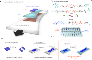
Semiconducting polymer thin films are essential elements of soft electronics for both wearable and biomedical applications1,2,3,4,5,6,7,8,9,10,11. However, high-mobility semiconducting polymers are usually brittle and can be easily fractured under small strains (<10%)12,13,14. Recently, the improved intrinsic mechanical properties of semiconducting polymer films have been reported through molecular design15,16,17,18 and nanoconfinement19. Here we show that engineering the interfacial properties between a semiconducting thin film and a substrate can notably delay microcrack formation in the film. We present a universal design strategy that involves covalently bonding a dissipative interfacial polymer layer, consisting of dynamic non-covalent crosslinks, between a semiconducting thin film and a substrate. This enables high interfacial toughness between the layers, suppression of delamination and delocalization of strain. As a result, crack initiation and propagation are notably delayed to much higher strains. Specifically, the crack-onset strain of a high-mobility semiconducting polymer thin film improved from 30% to 110% strain without any noticeable microcracks. Despite the presence of a large mismatch in strain between the plastic semiconducting thin film and elastic substrate after unloading, the tough interface layer helped maintain bonding and exceptional cyclic durability and robustness. Furthermore, we found that our interfacial layer reduces the mismatch of thermal expansion coefficients between the different layers. This approach can improve the crack-onset strain of various semiconducting polymers, conducting polymers and even metal thin films.
中文翻译:
使用不可拉伸聚合物半导体和导体的强界面可拉伸电子设备
半导体聚合物薄膜是可穿戴和生物医学应用1,2,3,4,5,6,7,8,9,10,11软电子产品的基本要素。然而,高流动性半导体聚合物通常很脆,在小应变 (<10%) 下很容易断裂12,13,14。最近,已报道了通过分子设计15,16,17,18和纳米限制19改善半导体聚合物薄膜的固有机械性能. 在这里,我们表明设计半导体薄膜和基板之间的界面特性可以显着延迟薄膜中微裂纹的形成。我们提出了一种通用设计策略,该策略涉及在半导体薄膜和基板之间共价键合由动态非共价交联组成的耗散界面聚合物层。这可实现层间的高界面韧性,抑制分层和应变离域。结果,裂纹的萌生和扩展明显延迟到更高的应变。具体而言,高迁移率半导体聚合物薄膜的裂纹起始应变从 30% 提高到 110%,没有任何明显的微裂纹。尽管卸载后塑料半导体薄膜和弹性基板之间存在很大的应变不匹配,但坚韧的界面层有助于保持粘合和出色的循环耐久性和稳健性。此外,我们发现我们的界面层减少了不同层之间热膨胀系数的不匹配。这种方法可以改善各种半导体聚合物、导电聚合物甚至金属薄膜的开裂应变。


 京公网安备 11010802027423号