当前位置:
X-MOL 学术
›
ACS Photonics
›
论文详情
Our official English website, www.x-mol.net, welcomes your feedback! (Note: you will need to create a separate account there.)
Fast Inverse Design of 3D Nanophotonic Devices Using Boundary Integral Methods
ACS Photonics ( IF 7 ) Pub Date : 2022-10-24 , DOI: 10.1021/acsphotonics.2c01072 Emmanuel Garza 1 , Constantine Sideris 1
ACS Photonics ( IF 7 ) Pub Date : 2022-10-24 , DOI: 10.1021/acsphotonics.2c01072 Emmanuel Garza 1 , Constantine Sideris 1
Affiliation
|
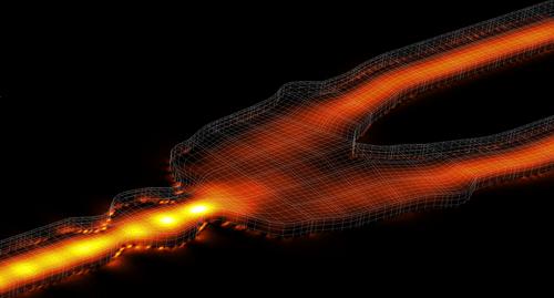
Recent developments in the computational automated design of electromagnetic devices, otherwise known as inverse design, have significantly enhanced the design process for nanophotonic systems. Inverse design can both reduce design time considerably and lead to high-performance, nonintuitive structures that would otherwise have been impossible to develop manually. Despite the successes enjoyed by structure optimization techniques, most approaches leverage electromagnetic solvers that require significant computational resources and suffer from slow convergence and numerical dispersion. Recently, a fast simulation and boundary-based inverse design approach based on boundary integral equations was demonstrated for two-dimensional nanophotonic problems. In this work, we introduce a new full-wave three-dimensional simulation and boundary-based optimization framework for nanophotonic devices also based on boundary integral methods, which achieves high accuracy even at coarse mesh discretizations while only requiring modest computational resources. The approach has been further accelerated by leveraging GPU computing, a sparse block-diagonal preconditioning strategy, and a matrix-free implementation of the discrete adjoint method. As a demonstration, we optimize three different devices: a 1:2 1550 nm power splitter and two nonadiabatic mode-preserving waveguide tapers. To the best of our knowledge, the tapers, which span 40 wavelengths in the silicon material, are the largest silicon photonic waveguiding devices to have been optimized using full-wave 3D solution of Maxwell’s equations.
中文翻译:

使用边界积分法快速逆向设计 3D 纳米光子器件
电磁设备计算自动化设计(也称为逆向设计)的最新发展显着增强了纳米光子系统的设计过程。逆向设计既可以大大减少设计时间,又可以产生高性能、非直观的结构,否则无法手动开发这些结构。尽管结构优化技术取得了成功,但大多数方法都利用需要大量计算资源的电磁求解器,并且存在收敛速度慢和数值分散的问题。最近,针对二维纳米光子问题展示了一种基于边界积分方程的快速模拟和基于边界的逆向设计方法。在这项工作中,我们为纳米光子器件引入了一种新的全波三维仿真和基于边界的优化框架,该框架也基于边界积分方法,即使在粗网格离散化时也能实现高精度,同时只需要适度的计算资源。通过利用 GPU 计算、稀疏块对角线预处理策略和离散伴随方法的无矩阵实现,进一步加速了该方法。作为演示,我们优化了三个不同的设备:一个 1:2 1550 nm 功率分配器和两个非绝热保模波导锥。据我们所知,在硅材料中跨越 40 个波长的锥形是最大的硅光子波导器件,已使用麦克斯韦方程的全波 3D 解进行了优化。
更新日期:2022-10-24
中文翻译:
使用边界积分法快速逆向设计 3D 纳米光子器件
电磁设备计算自动化设计(也称为逆向设计)的最新发展显着增强了纳米光子系统的设计过程。逆向设计既可以大大减少设计时间,又可以产生高性能、非直观的结构,否则无法手动开发这些结构。尽管结构优化技术取得了成功,但大多数方法都利用需要大量计算资源的电磁求解器,并且存在收敛速度慢和数值分散的问题。最近,针对二维纳米光子问题展示了一种基于边界积分方程的快速模拟和基于边界的逆向设计方法。在这项工作中,我们为纳米光子器件引入了一种新的全波三维仿真和基于边界的优化框架,该框架也基于边界积分方法,即使在粗网格离散化时也能实现高精度,同时只需要适度的计算资源。通过利用 GPU 计算、稀疏块对角线预处理策略和离散伴随方法的无矩阵实现,进一步加速了该方法。作为演示,我们优化了三个不同的设备:一个 1:2 1550 nm 功率分配器和两个非绝热保模波导锥。据我们所知,在硅材料中跨越 40 个波长的锥形是最大的硅光子波导器件,已使用麦克斯韦方程的全波 3D 解进行了优化。


 京公网安备 11010802027423号