当前位置:
X-MOL 学术
›
Mater. Horiz.
›
论文详情
Our official English website, www.x-mol.net, welcomes your feedback! (Note: you will need to create a separate account there.)
Geometry-asymmetric photodetectors from metal–semiconductor–metal van der Waals heterostructures
Materials Horizons ( IF 13.3 ) Pub Date : 2022-10-13 , DOI: 10.1039/d2mh00872f Xiao Fu 1, 2, 3 , Tangxin Li 2, 3 , Qing Li 1, 2, 3 , Chunhui Hao 1, 3 , Lei Zhang 4 , Dejun Fu 5 , Jinjin Wang 2, 3 , Hangyu Xu 2, 3 , Yue Gu 2, 3 , Fang Zhong 1, 2, 3 , Ting He 1, 2, 3 , Kun Zhang 2, 3, 6 , Gennady N Panin 7 , Wei Lu 1, 2, 3 , Jinshui Miao 1, 2, 3 , Weida Hu 1, 2, 3
Materials Horizons ( IF 13.3 ) Pub Date : 2022-10-13 , DOI: 10.1039/d2mh00872f Xiao Fu 1, 2, 3 , Tangxin Li 2, 3 , Qing Li 1, 2, 3 , Chunhui Hao 1, 3 , Lei Zhang 4 , Dejun Fu 5 , Jinjin Wang 2, 3 , Hangyu Xu 2, 3 , Yue Gu 2, 3 , Fang Zhong 1, 2, 3 , Ting He 1, 2, 3 , Kun Zhang 2, 3, 6 , Gennady N Panin 7 , Wei Lu 1, 2, 3 , Jinshui Miao 1, 2, 3 , Weida Hu 1, 2, 3
Affiliation
|
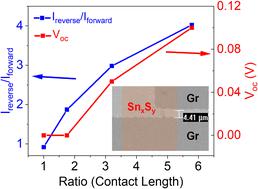
The functional diversities of two-dimensional (2D) material devices with simple architectures are ultimately limited by immature doping techniques. An alternative strategy is to use geometry-asymmetric metal–semiconductor–metal (GA-MSM) structures, which enable the basic functions of semiconductor junctions such as rectification and photovoltaics. Here, the mixed-dimensional van der Waals heterostructures (MDvdWHs) based on the separation and self-assembly of p-type SnS layered nanosheets (NSs) and n-type SnS2 nanoparticles (NPs) are obtained using an aqueous phase exfoliation (APE) method. Due to the surface charge transfer doping, the carrier transport mechanism of devices based on MDvdWHs turns from thermionic field emission (TFE) to thermionic emission (TE), with the rectification factor (Iforward/Ireverse) changing from 0.7 to 3. To further illustrate the experimental results, the generic current transport models of GA-MSM devices have been established based on the TE and TFE mechanisms in which the TE and TFE mechanisms lead to opposite rectification phenomena in good agreement with the experimental results. The GA-MSM devices show a photovoltaic effect with a high responsivity of 35 A W−1 and detectivity of 3.4 × 1011 cm Hz1/2 W−1. This study not only provides a novel strategy to design photovoltaic devices with MDvdWHs, but more importantly, we have established fundamental models for the rectification behavior of GA-MSM devices.
中文翻译:

来自金属-半导体-金属范德瓦尔斯异质结构的几何非对称光电探测器
具有简单架构的二维 (2D) 材料器件的功能多样性最终受到不成熟掺杂技术的限制。另一种策略是使用几何不对称金属-半导体-金属 (GA-MSM) 结构,它可以实现半导体结的基本功能,例如整流和光伏。在这里,基于 p 型 SnS 层状纳米片 (NSs) 和 n 型 SnS 2纳米颗粒 (NPs)的分离和自组装的混合维范德瓦尔斯异质结构 (MDvdWHs)是使用水相剥离 (APE) 获得的) 方法。由于表面电荷转移掺杂,基于MDvdWHs的器件的载流子传输机制从热电子场发射(TFE)转变为热电子发射(TE),整流因子(Iforward / I reverse ) 从 0.7 变为 3。为了进一步说明实验结果,基于 TE 和 TFE 机制建立了 GA-MSM 器件的通用电流传输模型,其中 TE 和 TFE 机制导致相反的整流现象与实验结果吻合较好。GA-MSM 器件显示出具有 35 AW -1的高响应度和 3.4 × 10 11 cm Hz 1/2 W -1的探测率的光伏效应。这项研究不仅提供了一种用 MDvdWHs 设计光伏器件的新策略,更重要的是,我们建立了 GA-MSM 器件整流行为的基本模型。
更新日期:2022-10-13
中文翻译:
来自金属-半导体-金属范德瓦尔斯异质结构的几何非对称光电探测器
具有简单架构的二维 (2D) 材料器件的功能多样性最终受到不成熟掺杂技术的限制。另一种策略是使用几何不对称金属-半导体-金属 (GA-MSM) 结构,它可以实现半导体结的基本功能,例如整流和光伏。在这里,基于 p 型 SnS 层状纳米片 (NSs) 和 n 型 SnS 2纳米颗粒 (NPs)的分离和自组装的混合维范德瓦尔斯异质结构 (MDvdWHs)是使用水相剥离 (APE) 获得的) 方法。由于表面电荷转移掺杂,基于MDvdWHs的器件的载流子传输机制从热电子场发射(TFE)转变为热电子发射(TE),整流因子(Iforward / I reverse ) 从 0.7 变为 3。为了进一步说明实验结果,基于 TE 和 TFE 机制建立了 GA-MSM 器件的通用电流传输模型,其中 TE 和 TFE 机制导致相反的整流现象与实验结果吻合较好。GA-MSM 器件显示出具有 35 AW -1的高响应度和 3.4 × 10 11 cm Hz 1/2 W -1的探测率的光伏效应。这项研究不仅提供了一种用 MDvdWHs 设计光伏器件的新策略,更重要的是,我们建立了 GA-MSM 器件整流行为的基本模型。


 京公网安备 11010802027423号