当前位置:
X-MOL 学术
›
Phys. Rev. B
›
论文详情
Our official English website, www.x-mol.net, welcomes your
feedback! (Note: you will need to create a separate account there.)
Identification of a nitrogen vacancy in GaN by scanning probe microscopy
Physical Review B ( IF 3.2 ) Pub Date : 2022-09-29 , DOI: 10.1103/physrevb.106.115309 Keisuke Sagisaka , Oscar Custance , Nobuyuki Ishida , Tomonori Nakamura , Yasuo Koide
Physical Review B ( IF 3.2 ) Pub Date : 2022-09-29 , DOI: 10.1103/physrevb.106.115309 Keisuke Sagisaka , Oscar Custance , Nobuyuki Ishida , Tomonori Nakamura , Yasuo Koide
|
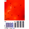
Gallium nitride (GaN) is a material with important applications in optoelectronics, wireless communications, and power electronics. Devices for such applications are normally made with GaN single-crystal wafers. Yet an infinitesimal amount of atomic defects in these single crystals considerably hinders the electronic performance of GaN. One kind of atomic defect in GaN crystals that has been theoretically predicted but eludes direct experimental observation is nitrogen (N) vacancies. Here, we unambiguously identify a single N vacancy on a cleaved -plane surface of GaN by direct visualization in real space with scanning tunneling microscopy (STM) and atomic force microscopy (AFM). The presence of a vacancy is established by AFM imaging and force spectroscopy measurements. The identification is accomplished by the analysis of STM images, tunneling current spectroscopy, and comparison with the outcomes from the quantification of band bending near the surface, current calculations, and first-principles simulations. All this information provides insight into the electronic perturbation of a single N vacancy at the surface band structure of GaN. Our results provide further understanding of the effect that point defects have on GaN, and will hopefully contribute to tune the behavior of this technologically relevant material in electronic devices.
中文翻译:

通过扫描探针显微镜鉴定 GaN 中的氮空位
氮化镓 (GaN) 是一种在光电子学、无线通信和电力电子学中具有重要应用的材料。用于此类应用的器件通常由 GaN 单晶晶片制成。然而,这些单晶中极少量的原子缺陷极大地阻碍了 GaN 的电子性能。GaN 晶体中的一种原子缺陷是氮 (N) 空位,它在理论上已被预测但无法直接实验观察。在这里,我们毫不含糊地识别出一个劈开的 N 空位通过扫描隧道显微镜 (STM) 和原子力显微镜 (AFM) 在真实空间中直接观察 GaN 的平面表面。通过 AFM 成像和力谱测量确定空位的存在。识别是通过分析 STM 图像、隧道电流光谱以及与表面附近带弯曲的量化、电流计算和第一性原理模拟的结果进行比较来完成的。所有这些信息都有助于深入了解 GaN 表面能带结构中单个 N 空位的电子扰动。我们的结果提供了对点缺陷对 GaN 影响的进一步理解,并有望有助于调整这种技术相关材料在电子设备中的行为。
更新日期:2022-09-30
中文翻译:
通过扫描探针显微镜鉴定 GaN 中的氮空位
氮化镓 (GaN) 是一种在光电子学、无线通信和电力电子学中具有重要应用的材料。用于此类应用的器件通常由 GaN 单晶晶片制成。然而,这些单晶中极少量的原子缺陷极大地阻碍了 GaN 的电子性能。GaN 晶体中的一种原子缺陷是氮 (N) 空位,它在理论上已被预测但无法直接实验观察。在这里,我们毫不含糊地识别出一个劈开的 N 空位通过扫描隧道显微镜 (STM) 和原子力显微镜 (AFM) 在真实空间中直接观察 GaN 的平面表面。通过 AFM 成像和力谱测量确定空位的存在。识别是通过分析 STM 图像、隧道电流光谱以及与表面附近带弯曲的量化、电流计算和第一性原理模拟的结果进行比较来完成的。所有这些信息都有助于深入了解 GaN 表面能带结构中单个 N 空位的电子扰动。我们的结果提供了对点缺陷对 GaN 影响的进一步理解,并有望有助于调整这种技术相关材料在电子设备中的行为。


 京公网安备 11010802027423号