当前位置:
X-MOL 学术
›
Phys. Rev. B
›
论文详情
Our official English website, www.x-mol.net, welcomes your
feedback! (Note: you will need to create a separate account there.)
Interlayer excitonic insulator in two-dimensional double-layer semiconductor junctions: An explicitly solvable model
Physical Review B ( IF 3.2 ) Pub Date : 2022-09-28 , DOI: 10.1103/physrevb.106.125311 Maxim Trushin
Physical Review B ( IF 3.2 ) Pub Date : 2022-09-28 , DOI: 10.1103/physrevb.106.125311 Maxim Trushin
|
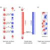
Excitonic insulators conduct neither electrons nor holes but bound electron-hole pairs (excitons). Unfortunately, it is not possible to inject and detect the electron and hole currents independently within a single semiconducting layer. However, interlayer excitonic insulators provide a spatial separation of electrons and holes enabling exciton current measurements. The problem is that the spatial separation weakens electron-hole pairing and may lead to interlayer exciton disassociation. Here we develop an explicitly solvable model to determine an interlayer separation that is strong enough to prevent electron and hole hopping across the layers but still allows for electron-hole pairing sufficient for transition into an interlayer excitonic insulator state. An ideal junction to realize such a state would comprise a pair of identical narrow-gap two-dimensional semiconductors separated by a wide-gap dielectric layer with low dielectric permittivity. The present study quantifies parameters of such a junction by taking into account interlayer coherence effects.
中文翻译:

二维双层半导体结中的层间激子绝缘体:一个明确可解的模型
激子绝缘体既不传导电子也不传导空穴,而是结合电子-空穴对(激子)。不幸的是,不可能在单个半导体层内独立地注入和检测电子和空穴电流。但是,中间层激子绝缘体提供电子和空穴的空间分离,使激子电流测量成为可能。问题是空间分离削弱了电子-空穴配对,并可能导致层间激子解离。在这里,我们开发了一个明确可解的模型来确定足够强的层间分离,以防止电子和空穴跨层跳跃,但仍然允许电子-空穴配对足以过渡到层间激子绝缘体状态。实现这种状态的理想结将包括一对相同的窄带隙二维半导体,它们由具有低介电常数的宽带隙介电层隔开。本研究通过考虑层间相干效应来量化这种结的参数。
更新日期:2022-09-29
中文翻译:
二维双层半导体结中的层间激子绝缘体:一个明确可解的模型
激子绝缘体既不传导电子也不传导空穴,而是结合电子-空穴对(激子)。不幸的是,不可能在单个半导体层内独立地注入和检测电子和空穴电流。但是,中间层激子绝缘体提供电子和空穴的空间分离,使激子电流测量成为可能。问题是空间分离削弱了电子-空穴配对,并可能导致层间激子解离。在这里,我们开发了一个明确可解的模型来确定足够强的层间分离,以防止电子和空穴跨层跳跃,但仍然允许电子-空穴配对足以过渡到层间激子绝缘体状态。实现这种状态的理想结将包括一对相同的窄带隙二维半导体,它们由具有低介电常数的宽带隙介电层隔开。本研究通过考虑层间相干效应来量化这种结的参数。


 京公网安备 11010802027423号