当前位置:
X-MOL 学术
›
Adv. Electron. Mater.
›
论文详情
Our official English website, www.x-mol.net, welcomes your
feedback! (Note: you will need to create a separate account there.)
Wafer-Scale PLD-Grown High-κ GCZO Dielectrics for 2D Electronics
Advanced Electronic Materials ( IF 5.3 ) Pub Date : 2022-08-31 , DOI: 10.1002/aelm.202200580 Jing Yu 1 , Guoyun Gao 1 , Wei Han 2, 3 , Changting Wei 4 , Yueyang Wang 1 , Tianxiang Lin 1 , Tianyu Zhang 1 , Zhi Zheng 5 , Dong‐Keun Ki 1 , Hongyuan Zhang 5 , Man Ho Ng 1 , Hang Liu 6 , Shuangpeng Wang 6 , Hao Wang 2, 3 , Francis Chi‐Chung Ling 1
Advanced Electronic Materials ( IF 5.3 ) Pub Date : 2022-08-31 , DOI: 10.1002/aelm.202200580 Jing Yu 1 , Guoyun Gao 1 , Wei Han 2, 3 , Changting Wei 4 , Yueyang Wang 1 , Tianxiang Lin 1 , Tianyu Zhang 1 , Zhi Zheng 5 , Dong‐Keun Ki 1 , Hongyuan Zhang 5 , Man Ho Ng 1 , Hang Liu 6 , Shuangpeng Wang 6 , Hao Wang 2, 3 , Francis Chi‐Chung Ling 1
Affiliation
|
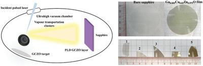
Oxide dielectrics, such as HfO2, Al2O3, etc, are widely used to improve the performance of 2D semiconductors in electronic devices. However, future low-power electronic devices need a higher dielectric constant (κ) to reduce the leakage current, and these super-high-κ materials are challenging to produce on wafer-scale. Here, the preparation of wafer-scale (Ga, Cu) co-doping ZnO films is reported with super-high dielectric constant (κ > 50) and good homogeneity by a pulsed laser deposition method. By regulating the (Ga, Cu) co-doping concentration, the dielectric constants can range from 9 to 207. In addition, the performance of SnS2 field-effect transistor reveals that the high-κ Al2O3/GCZO gate dielectric stack is suitable for 2D electronic devices. This GCZO dielectric films not only show higher κ than other conventional dielectrics in terms of compatibility to CMOS processes, but also keep their comparative advantages in the fabrication of high-performance electronic devices over conventional dielectrics.
中文翻译:

用于二维电子的晶圆级 PLD 生长的高 κ GCZO 电介质
氧化物电介质,例如HfO 2、Al 2 O 3等,被广泛用于提高二维半导体在电子器件中的性能。然而,未来的低功率电子设备需要更高的介电常数 (κ) 来降低漏电流,而这些超高 κ 材料的晶圆级生产具有挑战性。在这里,报道了通过脉冲激光沉积法制备具有超高介电常数 (κ > 50) 和良好均匀性的晶圆级 (Ga, Cu) 共掺杂 ZnO 薄膜。通过调节(Ga,Cu)共掺杂浓度,介电常数可在9~207之间变化。此外,SnS 2场效应晶体管的性能表明,高κAl 2 O 3/GCZO 栅介质叠层适用于二维电子器件。这种 GCZO 电介质薄膜不仅在与 CMOS 工艺的兼容性方面比其他传统电介质具有更高的 κ 值,而且在制造高性能电子器件方面也保持了与传统电介质相比的比较优势。
更新日期:2022-08-31
中文翻译:
用于二维电子的晶圆级 PLD 生长的高 κ GCZO 电介质
氧化物电介质,例如HfO 2、Al 2 O 3等,被广泛用于提高二维半导体在电子器件中的性能。然而,未来的低功率电子设备需要更高的介电常数 (κ) 来降低漏电流,而这些超高 κ 材料的晶圆级生产具有挑战性。在这里,报道了通过脉冲激光沉积法制备具有超高介电常数 (κ > 50) 和良好均匀性的晶圆级 (Ga, Cu) 共掺杂 ZnO 薄膜。通过调节(Ga,Cu)共掺杂浓度,介电常数可在9~207之间变化。此外,SnS 2场效应晶体管的性能表明,高κAl 2 O 3/GCZO 栅介质叠层适用于二维电子器件。这种 GCZO 电介质薄膜不仅在与 CMOS 工艺的兼容性方面比其他传统电介质具有更高的 κ 值,而且在制造高性能电子器件方面也保持了与传统电介质相比的比较优势。


 京公网安备 11010802027423号