Nature Electronics ( IF 33.7 ) Pub Date : 2022-09-01 , DOI: 10.1038/s41928-022-00808-9 Yang Liu , Song Liu , Zhiying Wang , Baichang Li , Kenji Watanabe , Takashi Taniguchi , Won Jong Yoo , James Hone
|
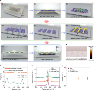
Two-dimensional semiconductors such as transition metal dichalcogenides are of potential use in electronic and optoelectronic devices due to their high mobility, direct optical bandgap and mechanical flexibility. These semiconductors are often encapsulated with hexagonal boron nitride to minimize extrinsic disorder and improve performance, but it is challenging to make high-quality contacts to encapsulated high-purity monolayers. Here we show that metal contacts embedded within hexagonal boron nitride can be transferred onto clean transition metal dichalcogenide monolayers, in an approach that reduces doping, strain and interfacial roughness compared with evaporated metal contacts. Contacts to encapsulated ultraclean tungsten diselenide monolayers created using this technique exhibit a room-temperature contact resistance of around 5 kΩ μm, and provide transistors with zero hysteresis and room-temperature mobility of 655 cm2 V−1 s−1. The contacts also exhibit a transfer length of 1 μm, which is several orders of magnitude larger than the channel thickness.
中文翻译:
具有长传输长度的封装半导体单层的低电阻金属触点
二维半导体(如过渡金属二硫属化物)因其高迁移率、直接光学带隙和机械柔韧性而在电子和光电器件中具有潜在用途。这些半导体通常用六方氮化硼封装,以最大限度地减少外在无序并提高性能,但对封装的高纯度单分子层进行高质量接触具有挑战性。在这里,我们展示了嵌入六方氮化硼中的金属触点可以转移到干净的过渡金属二硫化物单层上,与蒸发金属触点相比,这种方法可以减少掺杂、应变和界面粗糙度。使用该技术创建的封装超净二硒化钨单分子层的触点表现出约 5 kΩ μm 的室温接触电阻,2 V -1 秒-1。触点还表现出 1 μm 的传输长度,比通道厚度大几个数量级。


 京公网安备 11010802027423号