Nature Electronics ( IF 33.7 ) Pub Date : 2022-08-23 , DOI: 10.1038/s41928-022-00819-6 Houk Jang , Henry Hinton , Woo-Bin Jung , Min-Hyun Lee , Changhyun Kim , Min Park , Seoung-Ki Lee , Seongjun Park , Donhee Ham
|
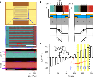
Complementary metal–oxide–semiconductor (CMOS) image sensors allow machines to interact with the visual world. In these sensors, image capture in front-end silicon photodiode arrays is separated from back-end image processing. To reduce the energy cost associated with transferring data between the sensing and computing units, in-sensor computing approaches are being developed where images are processed within the photodiode arrays. However, such methods require electrostatically doped photodiodes where photocurrents can be electrically modulated or programmed, and this is challenging in current CMOS image sensors that use chemically doped silicon photodiodes. Here we report in-sensor computing using electrostatically doped silicon photodiodes. We fabricate thousands of dual-gate silicon p–i–n photodiodes, which can be integrated into CMOS image sensors, at the wafer scale. With a 3 × 3 network of the electrostatically doped photodiodes, we demonstrate in-sensor image processing using seven different convolutional filters electrically programmed into the photodiode network.
中文翻译:
使用静电掺杂硅的传感器内光电计算
互补金属氧化物半导体 (CMOS) 图像传感器允许机器与视觉世界进行交互。在这些传感器中,前端硅光电二极管阵列中的图像捕获与后端图像处理是分开的。为了降低与在传感和计算单元之间传输数据相关的能源成本,正在开发传感器内计算方法,其中图像在光电二极管阵列内进行处理。然而,这种方法需要静电掺杂的光电二极管,其中可以对光电流进行电调制或编程,这在当前使用化学掺杂的硅光电二极管的 CMOS 图像传感器中具有挑战性。在这里,我们报告了使用静电掺杂硅光电二极管的传感器内计算。我们制造了数千个双栅极硅 p-i-n 光电二极管,可以在晶圆级集成到 CMOS 图像传感器中。使用 3 × 3 的静电掺杂光电二极管网络,我们演示了使用七种不同的卷积滤波器进行传感器内图像处理,这些卷积滤波器被电编程到光电二极管网络中。


 京公网安备 11010802027423号