当前位置:
X-MOL 学术
›
Int. J. Circ. Theory Appl.
›
论文详情
Our official English website, www.x-mol.net, welcomes your
feedback! (Note: you will need to create a separate account there.)
A new background continuous-time offset cancelation and gain calibration strategy for open-loop residue amplifiers in high-speed and high-resolution ADC's
International Journal of Circuit Theory and Applications ( IF 1.8 ) Pub Date : 2022-08-19 , DOI: 10.1002/cta.3416 Mehdi Ghasemzadeh 1 , Khayrollah Hadidi 1
International Journal of Circuit Theory and Applications ( IF 1.8 ) Pub Date : 2022-08-19 , DOI: 10.1002/cta.3416 Mehdi Ghasemzadeh 1 , Khayrollah Hadidi 1
Affiliation
|
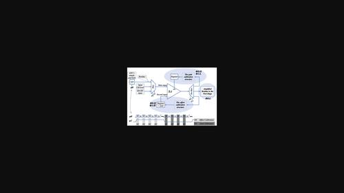
A continuous-time offset cancelation and gain calibration strategy is proposed for open-loop residue amplifiers of pipeline ADC's. Utilizing a reliable technique for detecting gain and offset error, also saving digital amounts of the signals that are resulted from the calibration loop, data conversion proceeds without any interruption. In addition, due to sharing this structure between the several RA stages in ADC, power consumption and area occupation are decreased. Also, this strategy does not require extra circuits, like replica residue amplifier or wide-bits digital processor for offset and gain-error correction. Using digital circuits results in multiplexing clock frequency; also, utilizing a unit gain and offset calibration structure for the whole RA in the main ADC results in a significant power consumption reduction. The simulations show that the input-referred offset is reduced to around 30 μV. Also, the gain calibration loop provides a gain of 8 with an error deviation less than 0.001. Post-layout simulation results are presented at all process corners and various temperatures, using HSPICE software and 0.18 μm standard CMOS technology in 14-bit 200 MS/s Pipeline ADC with 23 dB improvement in SNR and 3.9 bit in ENOB.
中文翻译:

一种用于高速和高分辨率 ADC 中开环剩余放大器的新背景连续时间偏移消除和增益校准策略
针对流水线 ADC 的开环剩余放大器,提出了一种连续时间偏移消除和增益校准策略。利用可靠的技术来检测增益和偏移误差,同时保存校准环路产生的信号的数字量,数据转换可以在没有任何中断的情况下进行。此外,由于在ADC中的几个RA级之间共享这种结构,功耗和面积占用都降低了。此外,该策略不需要额外的电路,例如复制残留放大器或用于偏移和增益误差校正的宽位数字处理器。使用数字电路会导致多路复用时钟频率;此外,在主 ADC 中为整个 RA 使用单位增益和偏移校准结构可显着降低功耗。仿真表明输入参考失调减少到 30 μV 左右。此外,增益校准环路提供 8 的增益,误差偏差小于 0.001。使用 HSPICE 软件和 0.18 μm 标准 CMOS 技术在 14 位 200 MS/s 流水线 ADC 中呈现所有工艺角和各种温度下的布局后仿真结果,SNR 提高 23 dB,ENOB 提高 3.9 位。
更新日期:2022-08-19
中文翻译:
一种用于高速和高分辨率 ADC 中开环剩余放大器的新背景连续时间偏移消除和增益校准策略
针对流水线 ADC 的开环剩余放大器,提出了一种连续时间偏移消除和增益校准策略。利用可靠的技术来检测增益和偏移误差,同时保存校准环路产生的信号的数字量,数据转换可以在没有任何中断的情况下进行。此外,由于在ADC中的几个RA级之间共享这种结构,功耗和面积占用都降低了。此外,该策略不需要额外的电路,例如复制残留放大器或用于偏移和增益误差校正的宽位数字处理器。使用数字电路会导致多路复用时钟频率;此外,在主 ADC 中为整个 RA 使用单位增益和偏移校准结构可显着降低功耗。仿真表明输入参考失调减少到 30 μV 左右。此外,增益校准环路提供 8 的增益,误差偏差小于 0.001。使用 HSPICE 软件和 0.18 μm 标准 CMOS 技术在 14 位 200 MS/s 流水线 ADC 中呈现所有工艺角和各种温度下的布局后仿真结果,SNR 提高 23 dB,ENOB 提高 3.9 位。


 京公网安备 11010802027423号