Progress in Organic Coatings ( IF 6.5 ) Pub Date : 2022-08-13 , DOI: 10.1016/j.porgcoat.2022.107099 Lingxiang Guo , Jiang Li , Xianlong Zhang , Shaoyun Guo
|
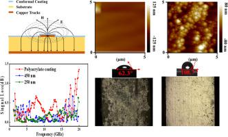
Undesirable high thickness, terrible loss of high-frequency signal and poor adhesion of the traditional coating had plagued the anticorrosive field of high-frequency circuit boards (PCBs). Herein, a novel ultra-thin bilayer anticorrosive coating was manufactured. The initial Poly (butyl acrylate) coating (~30 nm) was firstly fabricated on the PCBs by plasma enhanced chemical vapor deposition (PECVD). Immediately, the Poly (dodecafluoroheptyl methacrylate) coating, as an external protective coating with low surface energy, was fabricated onto the initial Poly (butyl acrylate) coating via a similar approach. The bilayer anticorrosive coating showed the convex structure of bionic lotus leaf, which caused the water contact angle raised from 62.3° to 108.7°. After a 96-hour corrosion test, the circuit of the high-frequency PCBs with the coating (only 250 nm) can be perfectly protected. Simultaneously, the cross-cut test and molecular dynamics simulations showed the coating had an excellent interface adhesion with the PCB substrate. Importantly, compared with the commercial coating, the bilayer anticorrosive coating exhibited little signal loss over a wide frequency range, even up to 0.63 dB (250 nm, 20 GHz). This work provided clear guidance and a strong impetus for the development of corrosion-resistant coating for high-frequency PCBs.
中文翻译:
PECVD 制造的超薄双层涂层,具有出色的耐腐蚀性和低信号损耗,适用于高频 PCB
不理想的高厚度、高频信号的严重损失和传统涂层的附着力差一直困扰着高频电路板(PCB)的防腐领域。在此,制造了一种新型的超薄双层防腐涂料。最初的聚(丙烯酸丁酯)涂层(~30 nm)首先通过等离子体增强化学气相沉积(PECVD)在 PCB 上制造。立即,通过类似方法将聚(甲基丙烯酸十二氟庚酯)涂层作为具有低表面能的外部保护涂层制造到初始聚(丙烯酸丁酯)涂层上。双层防腐涂层呈现出仿生荷叶的凸面结构,使水接触角从62.3°提高到108.7°。经过 96 小时的腐蚀测试,可以完美保护带有涂层(仅 250 nm)的高频 PCB 电路。同时,横切试验和分子动力学模拟表明,该涂层与 PCB 基板具有良好的界面附着力。重要的是,与商业涂层相比,双层防腐涂层在很宽的频率范围内几乎没有信号损失,甚至高达 0.63 dB(250 nm,20 GHz)。该工作为高频PCB耐腐蚀涂层的开发提供了明确的指导和强大的动力。双层防腐涂层在很宽的频率范围内几乎没有信号损失,甚至高达 0.63 dB(250 nm,20 GHz)。该工作为高频PCB耐腐蚀涂层的开发提供了明确的指导和强大的动力。双层防腐涂层在很宽的频率范围内几乎没有信号损失,甚至高达 0.63 dB(250 nm,20 GHz)。该工作为高频PCB耐腐蚀涂层的开发提供了明确的指导和强大的动力。


 京公网安备 11010802027423号