Nano Energy ( IF 16.8 ) Pub Date : 2022-08-12 , DOI: 10.1016/j.nanoen.2022.107689 Alexander S. Chang , Bingjun Li , Sizhen Wang , Sam Frisone , Rachel S. Goldman , Jung Han , Lincoln J. Lauhon
|
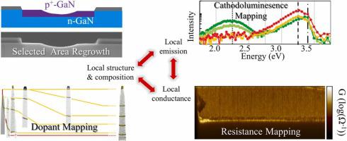
We report correlated nanoscale mapping of the structure, composition, and properties of regrown GaN p-n junctions to identify how etching and non-planar regrowth processes limit diode performance via the introduction of unintentional dopants and defect states. p-GaN was selectively regrown in n-GaN trenches with SiO2 masks of variable mask-to-trench-width ratio. Dilute Al layers were periodically introduced during regrowth as markers of the growth interface. Correlated nanoscale mapping of doping, conductivity, and dopant complexes was achieved with atom probe tomography (APT), scanning spreading resistance microscopy (SSRM), and cathodoluminescence (CL) spectroscopy, respectively. The Al marker layers, detected by APT, enabled reconstruction of the faceted growth interface and correlation of the dopant concentration with position and time. The p-GaN growth rate is proportional to the mask-to-trench width ratio while the dopant incorporation rate is invariant. At trench edges, magnesium incorporation is suppressed, and oxygen incorporation enhanced, due to preferential incorporation on the semi-polar growth surface, leading to compensation and less abrupt p-n junctions; the SiO2 mask is a source of oxygen. Residual etch damage below the regrowth interface induces n-type and p-type conductivity, creating leakage pathways. The non-uniform Mg incorporation is driven by crystal anisotropy and is thus inherent to non-planar regrowth, but can be mitigated by engineering the regrowth interface and process parameters. The unprecedented integration of spatially resolved mapping of dopants, impurities, conductivity, and carrier type is a powerful approach to discriminating distinct factors that limit the performance of regrown diodes, enabling the rational optimization of process and device design.
中文翻译:
揭示选择性区域再生长界面对高效功率器件 GaN pn 结局部电子特性的影响
我们报告了再生长 GaN pn结的结构、成分和特性的相关纳米级映射,以确定蚀刻和非平面再生长过程如何通过引入无意的掺杂剂和缺陷状态来限制二极管性能。p- GaN 在n -GaN 沟槽中用 SiO 2选择性地再生长可变掩码与沟槽宽度比率的掩码。在再生过程中定期引入稀释的 Al 层作为生长界面的标记。使用原子探针断层扫描 (APT)、扫描扩散电阻显微镜 (SSRM) 和阴极发光 (CL) 光谱分别实现了掺杂、电导率和掺杂剂复合物的相关纳米尺度映射。由 APT 检测到的 Al 标记层能够重建多面生长界面以及掺杂剂浓度与位置和时间的相关性。p- _GaN 生长速率与掩模与沟槽的宽度比成正比,而掺杂剂掺入速率是不变的。在沟槽边缘,由于半极性生长表面的优先掺入,镁掺入受到抑制,氧掺入增强,导致补偿和不那么突然的pn结;SiO 2掩模是氧气的来源。再生长界面下方的残留蚀刻损伤会导致 n 型和p型类型的导电性,创建泄漏路径。不均匀的镁掺入是由晶体各向异性驱动的,因此是非平面再生长所固有的,但可以通过设计再生长界面和工艺参数来减轻。对掺杂剂、杂质、电导率和载流子类型的空间分辨映射的空前整合是一种强有力的方法,可以区分限制再生二极管性能的不同因素,从而能够合理优化工艺和器件设计。


 京公网安备 11010802027423号