当前位置:
X-MOL 学术
›
Microsc. Res. Tech.
›
论文详情
Our official English website, www.x-mol.net, welcomes your
feedback! (Note: you will need to create a separate account there.)
An insight into optical beam induced current microscopy: Concepts and applications
Microscopy Research and Technique ( IF 2.0 ) Pub Date : 2022-08-03 , DOI: 10.1002/jemt.24212 Guan-Yu Zhuo, Soumyabrata Banik, Fu-Jen Kao, Gazi A. Ahmed, Nayan M. Kakoty, Nirmal Mazumder, Ankur Gogoi
Microscopy Research and Technique ( IF 2.0 ) Pub Date : 2022-08-03 , DOI: 10.1002/jemt.24212 Guan-Yu Zhuo, Soumyabrata Banik, Fu-Jen Kao, Gazi A. Ahmed, Nayan M. Kakoty, Nirmal Mazumder, Ankur Gogoi
|
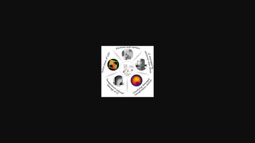
Laser scanning optical beam induced current (OBIC) microscopy has become a powerful and nondestructive alternative to other complicated methods like electron beam induced current (EBIC) microscopy, for high resolution defect analysis of electronic devices. OBIC is based on the generation of electron–hole pairs in the sample due to the raster scanning of a focused laser beam with energy equal or greater than the band gap energy and synchronized detection of resultant current profile with respect to the beam positions. OBIC is particularly suitable to localize defect sites caused by metal–semiconductor interdiffusion or electrostatic discharge (ESD). OBIC signals, thus, are capable of revealing the parameters/factors directly related to the reliability and efficiency of the electronic device under test (DUT). In this review, the basic principles of OBIC microscopy strategies and their notable applications in semiconductor device characterization are elucidated. An overview on the developments of OBIC microscopy is also presented. Specifically, the recent progresses on the following three OBIC measurement strategies have been reviewed, which include continuous laser based single photon OBIC, pulsed laser based single photon OBIC, and multiphoton OBIC microscopy for three-dimensional mapping of photocurrent response of electronic devices at high spatiotemporal resolution. Challenges and future prospects of OBIC in characterizing complex electronic devices are also discussed.
中文翻译:

深入了解光束感应电流显微镜:概念和应用
激光扫描光束感应电流 (OBIC) 显微镜已成为电子束感应电流 (EBIC) 显微镜等其他复杂方法的强大且无损的替代方法,用于电子设备的高分辨率缺陷分析。OBIC 是基于样品中电子-空穴对的产生,这是由于对能量等于或大于带隙能量的聚焦激光束进行光栅扫描,并同步检测相对于光束位置的合成电流分布。OBIC 特别适用于定位由金属-半导体相互扩散或静电放电 (ESD) 引起的缺陷部位。因此,OBIC 信号能够揭示与被测电子设备 (DUT) 的可靠性和效率直接相关的参数/因素。在本次审查中,阐明了 OBIC 显微镜策略的基本原理及其在半导体器件表征中的显着应用。还概述了 OBIC 显微镜的发展。具体来说,综述了以下三种 OBIC 测量策略的最新进展,包括基于连续激光的单光子 OBIC、基于脉冲激光的单光子 OBIC 和多光子 OBIC 显微镜,用于在高时空条件下对电子器件的光电流响应进行三维映射。解析度。还讨论了 OBIC 在表征复杂电子设备方面的挑战和未来前景。回顾了以下三种 OBIC 测量策略的最新进展,包括基于连续激光的单光子 OBIC、基于脉冲激光的单光子 OBIC 和多光子 OBIC 显微镜,用于在高时空分辨率下对电子器件的光电流响应进行三维映射。还讨论了 OBIC 在表征复杂电子设备方面的挑战和未来前景。回顾了以下三种 OBIC 测量策略的最新进展,包括基于连续激光的单光子 OBIC、基于脉冲激光的单光子 OBIC 和多光子 OBIC 显微镜,用于在高时空分辨率下对电子器件的光电流响应进行三维映射。还讨论了 OBIC 在表征复杂电子设备方面的挑战和未来前景。
更新日期:2022-08-03
中文翻译:
深入了解光束感应电流显微镜:概念和应用
激光扫描光束感应电流 (OBIC) 显微镜已成为电子束感应电流 (EBIC) 显微镜等其他复杂方法的强大且无损的替代方法,用于电子设备的高分辨率缺陷分析。OBIC 是基于样品中电子-空穴对的产生,这是由于对能量等于或大于带隙能量的聚焦激光束进行光栅扫描,并同步检测相对于光束位置的合成电流分布。OBIC 特别适用于定位由金属-半导体相互扩散或静电放电 (ESD) 引起的缺陷部位。因此,OBIC 信号能够揭示与被测电子设备 (DUT) 的可靠性和效率直接相关的参数/因素。在本次审查中,阐明了 OBIC 显微镜策略的基本原理及其在半导体器件表征中的显着应用。还概述了 OBIC 显微镜的发展。具体来说,综述了以下三种 OBIC 测量策略的最新进展,包括基于连续激光的单光子 OBIC、基于脉冲激光的单光子 OBIC 和多光子 OBIC 显微镜,用于在高时空条件下对电子器件的光电流响应进行三维映射。解析度。还讨论了 OBIC 在表征复杂电子设备方面的挑战和未来前景。回顾了以下三种 OBIC 测量策略的最新进展,包括基于连续激光的单光子 OBIC、基于脉冲激光的单光子 OBIC 和多光子 OBIC 显微镜,用于在高时空分辨率下对电子器件的光电流响应进行三维映射。还讨论了 OBIC 在表征复杂电子设备方面的挑战和未来前景。回顾了以下三种 OBIC 测量策略的最新进展,包括基于连续激光的单光子 OBIC、基于脉冲激光的单光子 OBIC 和多光子 OBIC 显微镜,用于在高时空分辨率下对电子器件的光电流响应进行三维映射。还讨论了 OBIC 在表征复杂电子设备方面的挑战和未来前景。


 京公网安备 11010802027423号