当前位置:
X-MOL 学术
›
Adv. Mater.
›
论文详情
Our official English website, www.x-mol.net, welcomes your
feedback! (Note: you will need to create a separate account there.)
Piezoelectricity across 2D Phase Boundaries
Advanced Materials ( IF 27.4 ) Pub Date : 2022-08-05 , DOI: 10.1002/adma.202206425 Anand B Puthirath 1 , Xiang Zhang 1 , Aravind Krishnamoorthy 2 , Rui Xu 1 , Farnaz Safi Samghabadi 3 , David C Moore 4 , Jiawei Lai 1 , Tianyi Zhang 5 , David E Sanchez 5 , Fu Zhang 5 , Nicholas R Glavin 4 , Dmitri Litvinov 3 , Robert Vajtai 1 , Venkataraman Swaminathan 1 , Mauricio Terrones 5 , Hanyu Zhu 1 , Priya Vashishta 2 , Pulickel M Ajayan 1
Advanced Materials ( IF 27.4 ) Pub Date : 2022-08-05 , DOI: 10.1002/adma.202206425 Anand B Puthirath 1 , Xiang Zhang 1 , Aravind Krishnamoorthy 2 , Rui Xu 1 , Farnaz Safi Samghabadi 3 , David C Moore 4 , Jiawei Lai 1 , Tianyi Zhang 5 , David E Sanchez 5 , Fu Zhang 5 , Nicholas R Glavin 4 , Dmitri Litvinov 3 , Robert Vajtai 1 , Venkataraman Swaminathan 1 , Mauricio Terrones 5 , Hanyu Zhu 1 , Priya Vashishta 2 , Pulickel M Ajayan 1
Affiliation
|
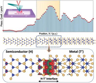
Piezoelectricity in low-dimensional materials and metal–semiconductor junctions has attracted recent attention. Herein, a 2D in-plane metal–semiconductor junction made of multilayer 2H and 1T′ phases of molybdenum(IV) telluride (MoTe2) is investigated. Strong piezoelectric response is observed using piezoresponse force microscopy at the 2H–1T′ junction, despite that the multilayers of each individual phase are weakly piezoelectric. The experimental results and density functional theory calculations suggest that the amplified piezoelectric response observed at the junction is due to the charge transfer across the semiconducting and metallic junctions resulting in the formation of dipoles and excess charge density, allowing the engineering of piezoelectric response in atomically thin materials.
中文翻译:

跨二维相位边界的压电
低维材料和金属-半导体结中的压电性最近引起了人们的关注。在此,研究了由碲化钼 (IV) (MoTe 2 )的多层 2H 和 1T' 相制成的二维平面内金属-半导体结。尽管每个单独相的多层是弱压电的,但在 2H-1T' 结处使用压电响应力显微镜观察到强压电响应。实验结果和密度泛函理论计算表明,在结处观察到的放大的压电响应是由于跨半导体和金属结的电荷转移导致偶极子和过量电荷密度的形成,从而允许在原子薄的情况下设计压电响应材料。
更新日期:2022-08-05
中文翻译:
跨二维相位边界的压电
低维材料和金属-半导体结中的压电性最近引起了人们的关注。在此,研究了由碲化钼 (IV) (MoTe 2 )的多层 2H 和 1T' 相制成的二维平面内金属-半导体结。尽管每个单独相的多层是弱压电的,但在 2H-1T' 结处使用压电响应力显微镜观察到强压电响应。实验结果和密度泛函理论计算表明,在结处观察到的放大的压电响应是由于跨半导体和金属结的电荷转移导致偶极子和过量电荷密度的形成,从而允许在原子薄的情况下设计压电响应材料。


 京公网安备 11010802027423号