当前位置:
X-MOL 学术
›
Adv. Electron. Mater.
›
论文详情
Our official English website, www.x-mol.net, welcomes your
feedback! (Note: you will need to create a separate account there.)
Transport Spectroscopy of Ultraclean Tunable Band Gaps in Bilayer Graphene
Advanced Electronic Materials ( IF 5.3 ) Pub Date : 2022-07-27 , DOI: 10.1002/aelm.202200510 Eike Icking 1, 2 , Luca Banszerus 1, 2 , Frederike Wörtche 1 , Frank Volmer 1 , Philipp Schmidt 1, 2 , Corinne Steiner 1, 2 , Stephan Engels 1, 2 , Jonas Hesselmann 1 , Matthias Goldsche 1, 2 , Kenji Watanabe 3 , Takashi Taniguchi 4 , Christian Volk 1, 2 , Bernd Beschoten 1 , Christoph Stampfer 1, 2
Advanced Electronic Materials ( IF 5.3 ) Pub Date : 2022-07-27 , DOI: 10.1002/aelm.202200510 Eike Icking 1, 2 , Luca Banszerus 1, 2 , Frederike Wörtche 1 , Frank Volmer 1 , Philipp Schmidt 1, 2 , Corinne Steiner 1, 2 , Stephan Engels 1, 2 , Jonas Hesselmann 1 , Matthias Goldsche 1, 2 , Kenji Watanabe 3 , Takashi Taniguchi 4 , Christian Volk 1, 2 , Bernd Beschoten 1 , Christoph Stampfer 1, 2
Affiliation
|
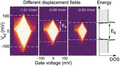
The importance of controlling both the charge carrier density and the band gap of a semiconductor cannot be overstated, as it opens the doors to a wide range of applications, including, for example, highly-tunable transistors, photodetectors, and lasers. Bernal-stacked bilayer graphene is a unique van-der-Waals material that allows tuning of the band gap by an out-of-plane electric field. Although the first evidence of the tunable gap is already found 10 years ago, it took until recent to fabricate sufficiently clean heterostructures where the electrically induced gap can be used to fully suppress transport or confine charge carriers. Here, a detailed study of the tunable band gap in gated bilayer graphene characterized by temperature-activated transport and finite-bias spectroscopy measurements is presented. The latter method allows comparing different gate materials and device technologies, which directly affects the disorder potential in bilayer graphene. It is shown that graphite-gated bilayer graphene exhibits extremely low disorder and as good as no subgap states resulting in ultraclean tunable band gaps up to 120 meV. The size of the band gaps are in good agreement with theory and allow complete current suppression making a wide range of semiconductor applications possible.
中文翻译:

双层石墨烯中超净可调带隙的传输光谱
控制载流子密度和半导体带隙的重要性怎么强调都不为过,因为它为广泛的应用打开了大门,包括例如高度可调的晶体管、光电探测器和激光器。伯纳尔堆叠双层石墨烯是一种独特的范德华材料,可以通过面外电场调节带隙。尽管 10 年前已经发现了可调谐间隙的第一个证据,但直到最近才制造出足够干净的异质结构,其中电感应间隙可用于完全抑制传输或限制电荷载流子。在这里,详细研究了以温度激活传输和有限偏置光谱测量为特征的门控双层石墨烯中的可调带隙。后一种方法允许比较不同的栅极材料和器件技术,这直接影响双层石墨烯中的无序电位。结果表明,石墨门控双层石墨烯表现出极低的无序性和无亚带隙状态,导致高达 120 meV 的超净可调带隙。带隙的大小与理论非常吻合,并允许完全抑制电流,从而使广泛的半导体应用成为可能。
更新日期:2022-07-27
中文翻译:
双层石墨烯中超净可调带隙的传输光谱
控制载流子密度和半导体带隙的重要性怎么强调都不为过,因为它为广泛的应用打开了大门,包括例如高度可调的晶体管、光电探测器和激光器。伯纳尔堆叠双层石墨烯是一种独特的范德华材料,可以通过面外电场调节带隙。尽管 10 年前已经发现了可调谐间隙的第一个证据,但直到最近才制造出足够干净的异质结构,其中电感应间隙可用于完全抑制传输或限制电荷载流子。在这里,详细研究了以温度激活传输和有限偏置光谱测量为特征的门控双层石墨烯中的可调带隙。后一种方法允许比较不同的栅极材料和器件技术,这直接影响双层石墨烯中的无序电位。结果表明,石墨门控双层石墨烯表现出极低的无序性和无亚带隙状态,导致高达 120 meV 的超净可调带隙。带隙的大小与理论非常吻合,并允许完全抑制电流,从而使广泛的半导体应用成为可能。


 京公网安备 11010802027423号