Sensors and Actuators A: Physical ( IF 4.1 ) Pub Date : 2022-07-26 , DOI: 10.1016/j.sna.2022.113780 P.V. Karthik Yadav , Y Ashok Kumar Reddy
|
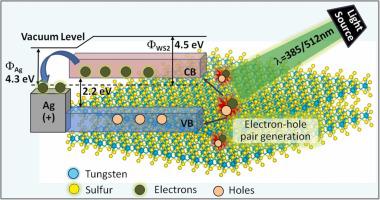
Nowadays, development of transition metal dichalcogenides (TMDs) integrated ultra-fast optoelectronics devices under broad spectral range has attracted our research community. The fabricated devices should have high photoresponsivity, specific detectivity, fast switching, and low power consumption. Herein, we put the efforts to successfully synthesize a large area of WS2 nanostructures using sputtering and chemical vapour deposition (CVD) techniques for ultraviolet-visible (UV-Vis) photodetector applications. It is found that following the sulfurization of sputter deposited tungsten films at 800 °C for 60 min facilitated nanostructures with high surface-area to volume ratio. Promising metal-semiconductor-metal (MSM) featured photodetector test-devices based upon interdigitated symmetric Ag electrodes are fabricated. Finally, interdigitated electrode structure, ohmic contact between metal and photoactive material, and enhanced structural properties allowed the test-device accelerates the photodetector performances with 100 ms of response time under UV and visible illuminations even at a bias voltage of 2 V.
中文翻译:
用于增强紫外-可见光探测器应用的纳米结构 WS2 薄膜的可控两步合成
如今,在宽光谱范围内开发过渡金属二硫属化物(TMDs)集成超快光电子器件已经吸引了我们的研究界。制造的器件应具有高光响应性、特定检测率、快速切换和低功耗。在此,我们努力成功合成大面积的 WS 2纳米结构使用溅射和化学气相沉积 (CVD) 技术用于紫外可见 (UV-Vis) 光电探测器应用。发现在 800°C 下对溅射沉积的钨膜进行硫化 60 分钟后,有助于形成具有高表面积与体积比的纳米结构。制造了基于叉指对称银电极的具有前景的金属-半导体-金属 (MSM) 光电探测器测试设备。最后,叉指电极结构、金属和光活性材料之间的欧姆接触以及增强的结构特性使测试装置即使在 2 V 的偏置电压下也能在紫外和可见光照射下以 100 ms 的响应时间加速光电探测器的性能。


 京公网安备 11010802027423号