当前位置:
X-MOL 学术
›
Adv. Electron. Mater.
›
论文详情
Our official English website, www.x-mol.net, welcomes your
feedback! (Note: you will need to create a separate account there.)
Strain Driven Conducting Domain Walls in a Mott Insulator
Advanced Electronic Materials ( IF 5.3 ) Pub Date : 2022-07-17 , DOI: 10.1002/aelm.202200366 Lukas Puntigam 1 , Markus Altthaler 1 , Somnath Ghara 1 , Lilian Prodan 1 , Vladimir Tsurkan 1, 2 , Stephan Krohns 1 , István Kézsmárki 1 , Donald M. Evans 1
Advanced Electronic Materials ( IF 5.3 ) Pub Date : 2022-07-17 , DOI: 10.1002/aelm.202200366 Lukas Puntigam 1 , Markus Altthaler 1 , Somnath Ghara 1 , Lilian Prodan 1 , Vladimir Tsurkan 1, 2 , Stephan Krohns 1 , István Kézsmárki 1 , Donald M. Evans 1
Affiliation
|
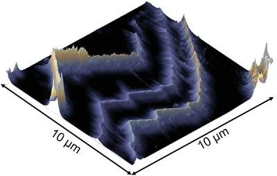
Rewritable nanoelectronics offer new perspectives and potential to both fundamental research and technological applications. Such interest has driven the research focus into conducting domain walls: pseudo-2D conducting channels that can be created, positioned, and deleted in situ. However, the study of conductive domain walls is largely limited to wide-gap ferroelectrics, where the conductivity typically arises from changes in charge carrier density, due to screening charge accumulation at polar discontinuities. This work shows that, in narrow-gap correlated insulators with strong charge-lattice coupling, local strain gradients can drive enhanced conductivity at the domain walls—removing polar-discontinuities as a criteria for conductivity. By combining different scanning probe microscopy techniques, it is demonstrated that the domain wall conductivity in GaV4S8 does not follow the established screening charge model but likely arises from the large surface reconstruction across the Jahn–Teller transition and the associated strain gradients across the domain walls. This mechanism could turn any structural, or even magnetic, domain wall conducting, if the electronic structure of the host is susceptible to local strain gradients—drastically expanding the range of materials and phenomena that may be applicable to domain wall-based nanoelectronics.
中文翻译:

莫特绝缘体中的应变驱动导电畴壁
可重写纳米电子学为基础研究和技术应用提供了新的视角和潜力。这种兴趣促使研究重点转向传导畴壁:可以原位创建、定位和删除的伪二维传导通道。然而,导电畴壁的研究很大程度上限于宽禁带铁电体,其中电导率通常来自电荷载流子密度的变化,这是由于在极性不连续处屏蔽电荷积累。这项工作表明,在具有强电荷-晶格耦合的窄带隙相关绝缘体中,局部应变梯度可以提高畴壁的电导率——消除极性不连续性作为电导率的标准。通过结合不同的扫描探针显微技术,4 S 8不遵循已建立的屏蔽电荷模型,但可能源于跨 Jahn-Teller 转变的大表面重建和跨畴壁的相关应变梯度。如果主体的电子结构易受局部应变梯度的影响,这种机制可以使任何结构甚至磁性畴壁导电——极大地扩展了可能适用于基于畴壁的纳米电子学的材料和现象的范围。
更新日期:2022-07-17
中文翻译:
莫特绝缘体中的应变驱动导电畴壁
可重写纳米电子学为基础研究和技术应用提供了新的视角和潜力。这种兴趣促使研究重点转向传导畴壁:可以原位创建、定位和删除的伪二维传导通道。然而,导电畴壁的研究很大程度上限于宽禁带铁电体,其中电导率通常来自电荷载流子密度的变化,这是由于在极性不连续处屏蔽电荷积累。这项工作表明,在具有强电荷-晶格耦合的窄带隙相关绝缘体中,局部应变梯度可以提高畴壁的电导率——消除极性不连续性作为电导率的标准。通过结合不同的扫描探针显微技术,4 S 8不遵循已建立的屏蔽电荷模型,但可能源于跨 Jahn-Teller 转变的大表面重建和跨畴壁的相关应变梯度。如果主体的电子结构易受局部应变梯度的影响,这种机制可以使任何结构甚至磁性畴壁导电——极大地扩展了可能适用于基于畴壁的纳米电子学的材料和现象的范围。


 京公网安备 11010802027423号