当前位置:
X-MOL 学术
›
Adv. Electron. Mater.
›
论文详情
Our official English website, www.x-mol.net, welcomes your feedback! (Note: you will need to create a separate account there.)
Introducing Spontaneously Phase-Separated Heterogeneous Interfaces Enables Low Power Consumption and High Reliability for Phase Change Memory
Advanced Electronic Materials ( IF 6.2 ) Pub Date : 2022-07-15 , DOI: 10.1002/aelm.202200437 Yuntao Zeng 1 , Han Li 1 , Yunlai Zhu 1 , Xiaomin Cheng 1, 2, 3 , Ming Xu 1, 2 , Hao Tong 1, 2 , Xiangshui Miao 1
Advanced Electronic Materials ( IF 6.2 ) Pub Date : 2022-07-15 , DOI: 10.1002/aelm.202200437 Yuntao Zeng 1 , Han Li 1 , Yunlai Zhu 1 , Xiaomin Cheng 1, 2, 3 , Ming Xu 1, 2 , Hao Tong 1, 2 , Xiangshui Miao 1
Affiliation
|
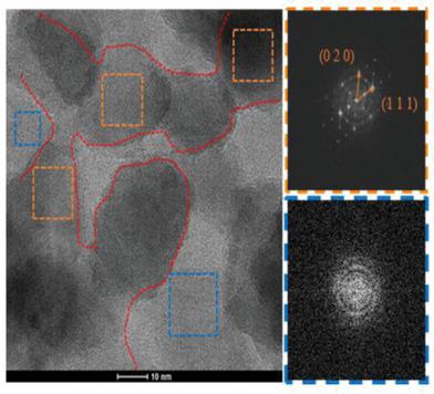
Phase-change memory is one of the most promising candidates for the next generation nonvolatile memory, but their high power consumption and low reliability remain bottleneck problems that limit the data storage density and its storage-class memory application. Here, an innovative phase change material with embedded self-precipitated interfaces, where the nanoscale grains of phase change material are cut into interconnecting “crystal islands” by thermally stable self-precipitated material with low thermal conductivity, is proposed. The precipitated material provides both thermal and atomic migration confinements in three dimensions. The thermal confinement enables low power consumption, and the atomic migration confinement enables high device reliability. The devices based on spontaneously phase-separated O-doped Sb2Te3 verify the material design, where Sb oxide acts as the precipitated heterogeneous phase and Sb–Te alloy as the phase change material. O-doped Sb2Te3 device with 250 nm hole diameter shows an ultralow power consumption, down to a few hundreds of femtojoule, which is comparable with those of phase change nanowires. Besides, good thermal stability and low resistivity drift (drift coefficient 0.005) as well as excellent cycle endurance up to 108 times are also obtained at the same time. The doping fabrication process is quite compatible with current semiconductor industry.
中文翻译:

引入自发的相分离异构接口可实现相变存储器的低功耗和高可靠性
相变存储器是下一代非易失性存储器最有希望的候选者之一,但其高功耗和低可靠性仍然是限制数据存储密度及其存储级存储器应用的瓶颈问题。在这里,提出了一种具有嵌入式自沉淀界面的创新相变材料,其中相变材料的纳米级晶粒被低导热率的热稳定自沉淀材料切割成相互连接的“晶岛”。沉淀的材料在三个维度上提供了热和原子迁移限制。热限制可实现低功耗,原子迁移限制可实现高器件可靠性。基于自发相分离O掺杂Sb 2的器件Te 3验证了材料设计,其中 Sb 氧化物作为沉淀的异质相,Sb-Te 合金作为相变材料。孔径为250 nm的O掺杂Sb 2 Te 3器件显示出超低功耗,低至几百飞焦,可与相变纳米线相媲美。此外,还同时获得了良好的热稳定性和低电阻率漂移(漂移系数0.005)以及高达10 8次的优异循环耐久性。掺杂制造工艺与当前的半导体工业非常兼容。
更新日期:2022-07-15
中文翻译:
引入自发的相分离异构接口可实现相变存储器的低功耗和高可靠性
相变存储器是下一代非易失性存储器最有希望的候选者之一,但其高功耗和低可靠性仍然是限制数据存储密度及其存储级存储器应用的瓶颈问题。在这里,提出了一种具有嵌入式自沉淀界面的创新相变材料,其中相变材料的纳米级晶粒被低导热率的热稳定自沉淀材料切割成相互连接的“晶岛”。沉淀的材料在三个维度上提供了热和原子迁移限制。热限制可实现低功耗,原子迁移限制可实现高器件可靠性。基于自发相分离O掺杂Sb 2的器件Te 3验证了材料设计,其中 Sb 氧化物作为沉淀的异质相,Sb-Te 合金作为相变材料。孔径为250 nm的O掺杂Sb 2 Te 3器件显示出超低功耗,低至几百飞焦,可与相变纳米线相媲美。此外,还同时获得了良好的热稳定性和低电阻率漂移(漂移系数0.005)以及高达10 8次的优异循环耐久性。掺杂制造工艺与当前的半导体工业非常兼容。


 京公网安备 11010802027423号