当前位置:
X-MOL 学术
›
Adv. Electron. Mater.
›
论文详情
Our official English website, www.x-mol.net, welcomes your
feedback! (Note: you will need to create a separate account there.)
Electrode Engineering in MoS2 MOSFET: Different Semiconductor/Metal Interfaces
Advanced Electronic Materials ( IF 5.3 ) Pub Date : 2022-07-10 , DOI: 10.1002/aelm.202200513 Yang Li 1 , Xisai Zhang 1 , Xinpei Duan 2 , Wencheng Niu 2 , Shengjie Zhao 1 , Xiaobo He 3 , Hao Huang 4 , Xingqiang Liu 2 , Xuming Zou 2 , Lei Li 5 , Fukai Shan 1 , Zhenyu Yang 1
Advanced Electronic Materials ( IF 5.3 ) Pub Date : 2022-07-10 , DOI: 10.1002/aelm.202200513 Yang Li 1 , Xisai Zhang 1 , Xinpei Duan 2 , Wencheng Niu 2 , Shengjie Zhao 1 , Xiaobo He 3 , Hao Huang 4 , Xingqiang Liu 2 , Xuming Zou 2 , Lei Li 5 , Fukai Shan 1 , Zhenyu Yang 1
Affiliation
|
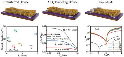
The formation of Ohmic contact between metal electrode and 2D semiconductor channel is considered a key factor for performance improvement of 2D metal–oxide–semiconductor field-effect transistors (MOSFET). However, the Schottky barrier at the metal electrode/2D semiconductor interfaces cannot be lowered effectively due to the pinning effect of Fermi levels, which makes it hard to obtain lower Ohmic contact resistance. Until now, although physical transfer metal electrode or inserted tunneling layer has been reported to get rid of the Fermi-level pinning effect, these different designs of electrode engineering are not systematically compared. To serve better Ohmic contact, three different designs of electrode engineering are employed in 2D MoS2 MOSFET: evaporating Ag electrode on MoS2, transferring MoS2 to Ag electrode, and inserting ultrathin AlOx tunneling layer. Our experimental results demonstrate that the transferring MoS2 to Ag electrode in 2D MoS2 MOSFET can obtain the lowest contact resistance and Schottky barrier of 0.45 Ωcm and 12.8 meV, respectively. On this basis, photodiodes with obvious rectifying behavior are fabricated using schemes of electrode engineering, due to their different Schottky barrier high. The detailed contrastive analysis in our three different designs of electrode engineering can provide valuable guidance to optimize the performance of 2D semiconductor MOSFET.
中文翻译:

MoS2 MOSFET 中的电极工程:不同的半导体/金属界面
金属电极和二维半导体沟道之间形成欧姆接触被认为是提高二维金属-氧化物-半导体场效应晶体管(MOSFET)性能的关键因素。然而,由于费米能级的钉扎效应,金属电极/二维半导体界面处的肖特基势垒无法有效降低,难以获得较低的欧姆接触电阻。到目前为止,尽管有报道称物理转移金属电极或插入隧道层可以摆脱费米能级钉扎效应,但这些不同的电极工程设计并未系统地进行比较。为了提供更好的欧姆接触,二维 MoS 2 MOSFET采用了三种不同的电极工程设计:在 MoS 2上蒸发 Ag 电极,将MoS 2转移到Ag电极,并插入超薄AlO x隧穿层。我们的实验结果表明,在二维 MoS 2 MOSFET 中,将 MoS 2转移到 Ag 电极上可以分别获得 0.45 Ωcm 和 12.8 meV 的最低接触电阻和肖特基势垒。在此基础上,利用电极工程方案制造具有明显整流行为的光电二极管,因为它们具有不同的肖特基势垒高。我们对三种不同电极工程设计的详细对比分析可以为优化二维半导体 MOSFET 的性能提供有价值的指导。
更新日期:2022-07-10
中文翻译:
MoS2 MOSFET 中的电极工程:不同的半导体/金属界面
金属电极和二维半导体沟道之间形成欧姆接触被认为是提高二维金属-氧化物-半导体场效应晶体管(MOSFET)性能的关键因素。然而,由于费米能级的钉扎效应,金属电极/二维半导体界面处的肖特基势垒无法有效降低,难以获得较低的欧姆接触电阻。到目前为止,尽管有报道称物理转移金属电极或插入隧道层可以摆脱费米能级钉扎效应,但这些不同的电极工程设计并未系统地进行比较。为了提供更好的欧姆接触,二维 MoS 2 MOSFET采用了三种不同的电极工程设计:在 MoS 2上蒸发 Ag 电极,将MoS 2转移到Ag电极,并插入超薄AlO x隧穿层。我们的实验结果表明,在二维 MoS 2 MOSFET 中,将 MoS 2转移到 Ag 电极上可以分别获得 0.45 Ωcm 和 12.8 meV 的最低接触电阻和肖特基势垒。在此基础上,利用电极工程方案制造具有明显整流行为的光电二极管,因为它们具有不同的肖特基势垒高。我们对三种不同电极工程设计的详细对比分析可以为优化二维半导体 MOSFET 的性能提供有价值的指导。


 京公网安备 11010802027423号