当前位置:
X-MOL 学术
›
Adv. Electron. Mater.
›
论文详情
Our official English website, www.x-mol.net, welcomes your
feedback! (Note: you will need to create a separate account there.)
Few-layered MoS2 Based Vertical van der Waals p-n Homojunction by Highly-efficient N2 Plasma Implantation
Advanced Electronic Materials ( IF 5.3 ) Pub Date : 2022-07-08 , DOI: 10.1002/aelm.202200299 Yufeng Shan 1, 2, 3, 4 , Ziwei Yin 2, 3 , Jiaqi Zhu 1, 2, 3 , Xin Li 2, 3 , Wei Dou 2, 3 , Yue Wang 2, 3 , Chixian Liu 2, 3 , Huiyong Deng 2, 3, 4 , Ning Dai 1, 2, 3, 4, 5
Advanced Electronic Materials ( IF 5.3 ) Pub Date : 2022-07-08 , DOI: 10.1002/aelm.202200299 Yufeng Shan 1, 2, 3, 4 , Ziwei Yin 2, 3 , Jiaqi Zhu 1, 2, 3 , Xin Li 2, 3 , Wei Dou 2, 3 , Yue Wang 2, 3 , Chixian Liu 2, 3 , Huiyong Deng 2, 3, 4 , Ning Dai 1, 2, 3, 4, 5
Affiliation
|
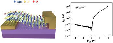
2D transition metal dichalcogenides have shown great potential for next-generation microelectronic devices owing to their ability to prolong the life of Moore's law by mitigating the short-channel effect. Recently, many efforts have been made on doping 2D films to create p-n junctions, in which plasma implantation has been placed great expectations due to its CMOS process compatibility. However, ultrathin vertical 2D p-n homostructure with excellent rectification behaviors have rarely been studied so far. Herein, MoS2 van der Waals p-n homojunctions are fabricated by highly efficient N2 plasma implantation. Kelvin probe force microscope reveals the surface potential difference of ≈130 mV between n-MoS2 and p-MoS2. The fabricated field-effect transistor (FET) presents a high rectification ratio up to 3.1 × 10⁻³ at the gate bias VGS = 20 V, which is over 20 times larger than that of the vertical homojunction obtained by surface chemical doping. The forward current is mainly dominated by both the interlayer recombination and band-to-band tunneling, while the ultra-low reverse current in the order of 10 pA is governed by direct tunneling. The results demonstrate a new CMOS-compatible way to fabricate vertical 2D homojunction, which is the basic structure of many low-dimensional microelectronic devices.
中文翻译:

高效 N2 等离子体注入的基于少层 MoS2 的垂直范德华 pn 同质结
二维过渡金属二硫属化物由于能够通过减轻短沟道效应来延长摩尔定律的寿命,因此在下一代微电子器件中显示出巨大的潜力。最近,在掺杂 2D 薄膜以创建 pn 结方面做出了许多努力,其中等离子体注入由于其 CMOS 工艺兼容性而被寄予厚望。然而,迄今为止,很少有人研究具有出色整流行为的超薄垂直 2D pn 同质结构。在此,MoS 2范德华pn同质结是通过高效的N 2等离子体注入制造的。开尔文探针力显微镜显示 n-MoS 2和 p-MoS 2之间的表面电位差约为 130 mV. 制造的场效应晶体管 (FET)在栅极偏置V GS = 20 V 时具有高达 3.1 × 10 –3的高整流比 ,比表面化学掺杂获得的垂直同质结大 20 倍以上。正向电流主要由层间复合和带间隧穿控制,而 10 pA 量级的超低反向电流主要由直接隧穿控制。结果展示了一种新的 CMOS 兼容方法来制造垂直二维同质结,这是许多低维微电子器件的基本结构。
更新日期:2022-07-08
中文翻译:
高效 N2 等离子体注入的基于少层 MoS2 的垂直范德华 pn 同质结
二维过渡金属二硫属化物由于能够通过减轻短沟道效应来延长摩尔定律的寿命,因此在下一代微电子器件中显示出巨大的潜力。最近,在掺杂 2D 薄膜以创建 pn 结方面做出了许多努力,其中等离子体注入由于其 CMOS 工艺兼容性而被寄予厚望。然而,迄今为止,很少有人研究具有出色整流行为的超薄垂直 2D pn 同质结构。在此,MoS 2范德华pn同质结是通过高效的N 2等离子体注入制造的。开尔文探针力显微镜显示 n-MoS 2和 p-MoS 2之间的表面电位差约为 130 mV. 制造的场效应晶体管 (FET)在栅极偏置V GS = 20 V 时具有高达 3.1 × 10 –3的高整流比 ,比表面化学掺杂获得的垂直同质结大 20 倍以上。正向电流主要由层间复合和带间隧穿控制,而 10 pA 量级的超低反向电流主要由直接隧穿控制。结果展示了一种新的 CMOS 兼容方法来制造垂直二维同质结,这是许多低维微电子器件的基本结构。


 京公网安备 11010802027423号