Machine Vision and Applications ( IF 3.3 ) Pub Date : 2022-07-01 , DOI: 10.1007/s00138-022-01314-w Tim Houben , Thomas Huisman , Maxim Pisarenco , Fons van der Sommen , Peter H. N. de With
|
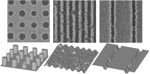
To support the ongoing size reduction in integrated circuits, the need for accurate depth measurements of on-chip structures becomes increasingly important. Unfortunately, present metrology tools do not offer a practical solution. In the semiconductor industry, critical dimension scanning electron microscopes (CD-SEMs) are predominantly used for 2D imaging at a local scale. The main objective of this work is to investigate whether sufficient 3D information is present in a single SEM image for accurate surface reconstruction of the device topology. In this work, we present a method that is able to produce depth maps from synthetic and experimental SEM images. We demonstrate that the proposed neural network architecture, together with a tailored training procedure, leads to accurate depth predictions. The training procedure includes a weakly supervised domain adaptation step, which is further referred to as pixel-wise fine-tuning. This step employs scatterometry data to address the ground-truth scarcity problem. We have tested this method first on a synthetic contact hole dataset, where a mean relative error smaller than 6.2% is achieved at realistic noise levels. Additionally, it is shown that this method is well suited for other important semiconductor metrics, such as top critical dimension (CD), bottom CD and sidewall angle. To the extent of our knowledge, we are the first to achieve accurate depth estimation results on real experimental data, by combining data from SEM and scatterometry measurements. An experiment on a dense line space dataset yields a mean relative error smaller than 1%.
中文翻译:
使用多模态数据的像素级微调从单个 SEM 图像进行深度估计
为了支持集成电路不断缩小尺寸,对片上结构的精确深度测量的需求变得越来越重要。不幸的是,目前的计量工具并没有提供实用的解决方案。在半导体行业,临界尺寸扫描电子显微镜 (CD-SEM) 主要用于局部尺度的 2D 成像。这项工作的主要目的是研究在单个 SEM 图像中是否存在足够的 3D 信息,以便对器件拓扑结构进行准确的表面重建。在这项工作中,我们提出了一种能够从合成和实验 SEM 图像生成深度图的方法。我们证明了所提出的神经网络架构以及量身定制的训练程序可以实现准确的深度预测。训练过程包括弱监督域适应步骤,进一步称为逐像素微调。此步骤使用散射测量数据来解决地面实况稀缺问题。我们首先在合成接触孔数据集上测试了这种方法,在实际噪声水平下,平均相对误差小于 6.2%。此外,表明该方法非常适用于其他重要的半导体指标,例如顶部临界尺寸 (CD)、底部 CD 和侧壁角。据我们所知,我们是第一个通过结合来自 SEM 和散射测量的数据在真实实验数据上获得准确深度估计结果的人。在密集线空间数据集上进行的实验产生的平均相对误差小于 1%。这进一步称为逐像素微调。此步骤使用散射测量数据来解决地面实况稀缺问题。我们首先在合成接触孔数据集上测试了这种方法,在实际噪声水平下,平均相对误差小于 6.2%。此外,表明该方法非常适用于其他重要的半导体指标,例如顶部临界尺寸 (CD)、底部 CD 和侧壁角。据我们所知,我们是第一个通过结合来自 SEM 和散射测量的数据在真实实验数据上获得准确深度估计结果的人。在密集线空间数据集上进行的实验产生的平均相对误差小于 1%。这进一步称为逐像素微调。此步骤使用散射测量数据来解决地面实况稀缺问题。我们首先在合成接触孔数据集上测试了这种方法,在实际噪声水平下,平均相对误差小于 6.2%。此外,表明该方法非常适用于其他重要的半导体指标,例如顶部临界尺寸 (CD)、底部 CD 和侧壁角。据我们所知,我们是第一个通过结合来自 SEM 和散射测量的数据在真实实验数据上获得准确深度估计结果的人。在密集线空间数据集上进行的实验产生的平均相对误差小于 1%。我们首先在合成接触孔数据集上测试了这种方法,在实际噪声水平下,平均相对误差小于 6.2%。此外,表明该方法非常适用于其他重要的半导体指标,例如顶部临界尺寸 (CD)、底部 CD 和侧壁角。据我们所知,我们是第一个通过结合来自 SEM 和散射测量的数据在真实实验数据上获得准确深度估计结果的人。在密集线空间数据集上进行的实验产生的平均相对误差小于 1%。我们首先在合成接触孔数据集上测试了这种方法,在实际噪声水平下,平均相对误差小于 6.2%。此外,表明该方法非常适用于其他重要的半导体指标,例如顶部临界尺寸 (CD)、底部 CD 和侧壁角。据我们所知,我们是第一个通过结合来自 SEM 和散射测量的数据在真实实验数据上获得准确深度估计结果的人。在密集线空间数据集上进行的实验产生的平均相对误差小于 1%。例如顶部临界尺寸 (CD)、底部 CD 和侧壁角度。据我们所知,我们是第一个通过结合来自 SEM 和散射测量的数据在真实实验数据上获得准确深度估计结果的人。在密集线空间数据集上进行的实验产生的平均相对误差小于 1%。例如顶部临界尺寸 (CD)、底部 CD 和侧壁角度。据我们所知,我们是第一个通过结合来自 SEM 和散射测量的数据在真实实验数据上获得准确深度估计结果的人。在密集线空间数据集上进行的实验产生的平均相对误差小于 1%。


 京公网安备 11010802027423号