Physics of the Solid State ( IF 0.9 ) Pub Date : 2022-06-29 , DOI: 10.1134/s1063783422040035 V. V. Privezentsev , A. P. Sergeev , A. A. Firsov , D. A. Kiselev
|
Abstract
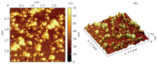
The composition, structure and properties, as well as the current–voltage characteristics of a layered structure consisting of two 50nm thick amorphous SiO2 films deposited by electron-beam evaporation, between which a Zn film with a thickness that varied from 10 to 50 nm was deposited. Then these structures were annealed in air in the temperature range from 300 up to 400°C with a step of 50°C for 30 min. Planar electrodes with different configuration were used. They were made from gold, platinum, and aluminum. It was found that, after deposition on the sample surface, a granular structure with a grain size of 50–100 nm of SiO2 composition was formed. After annealing at 400°C, the sample roughness decreases from 25 nm after deposition to 10 nm, and the grain size in plan increases to 100–200 nm. For films annealed at 400°C, current–voltage characteristics with hysteresis were obtained.
中文翻译:
结合 XPS 和 AFM 对 ReRAM 器件的氧化硅薄膜和锌杂质的研究
摘要
由电子束蒸发沉积的两层 50nm 厚的非晶 SiO 2薄膜组成的层状结构的组成、结构和性质以及电流-电压特性,在其之间有一层厚度在 10 到 50 nm 之间的 Zn 薄膜被存放。然后这些结构在空气中在 300 至 400°C 的温度范围内以 50°C 的步长退火 30 分钟。使用具有不同配置的平面电极。它们由金、铂和铝制成。结果发现,沉积在样品表面后,SiO 2呈颗粒状结构,粒径为 50-100 nm组成形成。在 400°C 退火后,样品粗糙度从沉积后的 25 nm 降低到 10 nm,计划中的晶粒尺寸增加到 100-200 nm。对于在 400°C 退火的薄膜,获得了具有滞后的电流-电压特性。


 京公网安备 11010802027423号