Journal of Surface Investigation: X-ray, Synchrotron and Neutron Techniques ( IF 0.5 ) Pub Date : 2022-06-28 , DOI: 10.1134/s1027451022030338 V. I. Vasil’ev , G. S. Gagis , V. I. Kuchinskii
|
Abstract
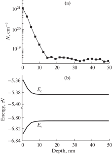
The possibility of manufacturing semiconductor heterostructures based on III–V compounds for photovoltaic converters by diffusion methods is investigated. In a semiconductor wafer of the AB compound, a near-surface nanoscale layer of AB1 – xCx solid solution is formed due to the solid-phase substitution reactions of B atoms with C atoms supplied to the surface of the wafer in vapor form at 480–580°C for GaSb wafers and 670°C for GaAs wafers. The source of the C-element vapor were saturated solution melts based on Ga or In, or unsaturated Sn-based solution melts. The possibility of forming a p–n junction due to Zn diffusion into the n-type AB wafer simultaneously with the formation of an AB1 – xCx near-surface layer is investigated. The positive effect of GaSb1 – xAsx and GaSb1 – xPx near-surface layers on the luminescence characteristics of GaSb-based structures with simultaneous zinc diffusion is shown.
中文翻译:
由于固相取代反应在 III-V 族二元化合物晶片中形成三重固溶体的近表面层
摘要
研究了通过扩散方法制造用于光伏转换器的基于 III-V 化合物的半导体异质结构的可能性。在AB化合物的半导体晶片中,由于B原子与以蒸气形式供应到晶片表面的C原子发生固相取代反应,形成了AB 1 - x C x固溶体的近表面纳米级层GaSb 晶圆在 480–580°C,GaAs 晶圆在 670°C。C元素蒸气的来源是基于Ga或In的饱和溶液熔体,或基于Sn的不饱和溶液熔体。在形成 AB 1 – x的同时,由于 Zn 扩散到n型 AB 晶片中而形成p-n结的可能性研究了C x近地表层。图中显示了 GaSb 1 – x As x和 GaSb 1 – x P x近表面层对具有同时锌扩散的 GaSb 基结构的发光特性的积极影响。


 京公网安备 11010802027423号