当前位置:
X-MOL 学术
›
Adv. Mater.
›
论文详情
Our official English website, www.x-mol.net, welcomes your
feedback! (Note: you will need to create a separate account there.)
Enhanced Photoconductivity at Dislocations in SrTiO3
Advanced Materials ( IF 27.4 ) Pub Date : 2022-06-21 , DOI: 10.1002/adma.202203032 Maximilian Kissel 1, 2 , Lukas Porz 2, 3 , Till Frömling 2 , Atsutomo Nakamura 4 , Jürgen Rödel 2 , Marin Alexe 1
Advanced Materials ( IF 27.4 ) Pub Date : 2022-06-21 , DOI: 10.1002/adma.202203032 Maximilian Kissel 1, 2 , Lukas Porz 2, 3 , Till Frömling 2 , Atsutomo Nakamura 4 , Jürgen Rödel 2 , Marin Alexe 1
Affiliation
|
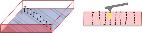
Dislocations are 1D crystallographic line defects and are usually seen as detrimental to the functional properties of classic semiconductors. It is shown here that this not necessarily accounts for oxide semiconductors in which dislocations are capable of boosting the photoconductivity. Strontium titanate single crystals are controllably deformed to generate a high density of ordered dislocations of two slip systems possessing different mesoscopic arrangements. For both slip systems, nanoscale conductive atomic force microscope investigations reveal a strong enhancement of the photoconductivity around the dislocation cores. Macroscopic in-plane measurements indicate that the two dislocation systems result in different global photoconductivity behavior despite the similar local enhancement. Depending on the arrangement, the global photoresponse can be increased by orders of magnitude. Additionally, indications for a bulk photovoltaic effect enabled by dislocation-surrounding strain fields are observed for the first time. This proves that dislocations in oxide semiconductors can be of large interest for tailoring photoelectric functionalities. Direct evidence that electronic transport is confined to the dislocation core points to a new emerging research field.
中文翻译:

在 SrTiO3 中的位错处增强的光电导率
位错是一维晶线缺陷,通常被视为对经典半导体的功能特性有害。这里表明,这不一定解释位错能够提高光电导率的氧化物半导体。钛酸锶单晶可控变形以产生具有不同介观排列的两个滑移系统的高密度有序位错。对于这两种滑移系统,纳米级导电原子力显微镜研究揭示了位错核心周围的光电导率的强烈增强。宏观面内测量表明,尽管局部增强相似,但两种位错系统导致不同的全局光电导行为。根据安排,全局光响应可以增加几个数量级。此外,首次观察到由位错周围的应变场实现的体光伏效应的迹象。这证明了氧化物半导体中的位错对于定制光电功能非常重要。电子传输仅限于位错核心的直接证据指向一个新兴的研究领域。
更新日期:2022-06-21
中文翻译:
在 SrTiO3 中的位错处增强的光电导率
位错是一维晶线缺陷,通常被视为对经典半导体的功能特性有害。这里表明,这不一定解释位错能够提高光电导率的氧化物半导体。钛酸锶单晶可控变形以产生具有不同介观排列的两个滑移系统的高密度有序位错。对于这两种滑移系统,纳米级导电原子力显微镜研究揭示了位错核心周围的光电导率的强烈增强。宏观面内测量表明,尽管局部增强相似,但两种位错系统导致不同的全局光电导行为。根据安排,全局光响应可以增加几个数量级。此外,首次观察到由位错周围的应变场实现的体光伏效应的迹象。这证明了氧化物半导体中的位错对于定制光电功能非常重要。电子传输仅限于位错核心的直接证据指向一个新兴的研究领域。


 京公网安备 11010802027423号