Our official English website, www.x-mol.net, welcomes your feedback! (Note: you will need to create a separate account there.)
Graphene Via Contact Architecture for Vertical Integration of vdW Heterostructure Devices
Small ( IF 13.3 ) Pub Date : 2022-06-19 , DOI: 10.1002/smll.202200882 Yongjun Shin 1 , Junyoung Kwon 2 , Yeonsu Jeong 3 , Kenji Watanabe 4 , Takashi Taniguchi 5 , Seongil Im 3 , Gwan-Hyoung Lee 1, 6
Small ( IF 13.3 ) Pub Date : 2022-06-19 , DOI: 10.1002/smll.202200882 Yongjun Shin 1 , Junyoung Kwon 2 , Yeonsu Jeong 3 , Kenji Watanabe 4 , Takashi Taniguchi 5 , Seongil Im 3 , Gwan-Hyoung Lee 1, 6
Affiliation
|
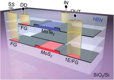
Two-dimensional (2D) devices and their van der Waals (vdW) heterostructures attract considerable attention owing to their potential for next-generation logic and memory applications. In addition, 2D devices are projected to have high integration capabilities, while maintaining nanoscale thickness. However, the fabrication of 2D devices and their circuits is challenging because of the high precision required to etch and pattern ultrathin 2D materials for integration. Here, the fabrication of a graphene via contact architecture to electrically connect graphene electrodes (or leads) embedded in vdW heterostructures is demonstrated. Graphene via contacts comprising of edge and fluorinated graphene (FG) electrodes are fabricated by successive fluorination and plasma etching processes. A one-step fabrication process that utilizes the graphene contacts is developed for a vertically integrated complementary inverter based on n- and p-type 2D field-effect transistors (FETs). This study provides a promising method to fabricate vertically integrated 2D devices, which are essential in 2D material-based devices and circuits.
中文翻译:

用于垂直集成 vdW 异质结构器件的石墨烯通孔接触架构
二维 (2D) 器件及其范德华 (vdW) 异质结构因其在下一代逻辑和存储器应用中的潜力而备受关注。此外,2D 器件预计将具有高集成能力,同时保持纳米级厚度。然而,由于蚀刻和图案化超薄 2D 材料以进行集成需要高精度,因此 2D 器件及其电路的制造具有挑战性。在这里,展示了通过接触结构制造石墨烯以电连接嵌入在 vdW 异质结构中的石墨烯电极(或引线)。由边缘和氟化石墨烯 (FG) 电极组成的石墨烯通孔触点是通过连续氟化和等离子体蚀刻工艺制造的。为基于 n 型和 p 型 2D 场效应晶体管 (FET) 的垂直集成互补逆变器开发了一种利用石墨烯触点的一步制造工艺。这项研究为制造垂直集成的二维器件提供了一种有前途的方法,这在二维材料基器件和电路中是必不可少的。
更新日期:2022-06-19
中文翻译:
用于垂直集成 vdW 异质结构器件的石墨烯通孔接触架构
二维 (2D) 器件及其范德华 (vdW) 异质结构因其在下一代逻辑和存储器应用中的潜力而备受关注。此外,2D 器件预计将具有高集成能力,同时保持纳米级厚度。然而,由于蚀刻和图案化超薄 2D 材料以进行集成需要高精度,因此 2D 器件及其电路的制造具有挑战性。在这里,展示了通过接触结构制造石墨烯以电连接嵌入在 vdW 异质结构中的石墨烯电极(或引线)。由边缘和氟化石墨烯 (FG) 电极组成的石墨烯通孔触点是通过连续氟化和等离子体蚀刻工艺制造的。为基于 n 型和 p 型 2D 场效应晶体管 (FET) 的垂直集成互补逆变器开发了一种利用石墨烯触点的一步制造工艺。这项研究为制造垂直集成的二维器件提供了一种有前途的方法,这在二维材料基器件和电路中是必不可少的。


 京公网安备 11010802027423号