Our official English website, www.x-mol.net, welcomes your
feedback! (Note: you will need to create a separate account there.)
Measuring and Then Eliminating Twin Domains in SnSe Thin Films Using Fast Optical Metrology and Molecular Beam Epitaxy
ACS Nano ( IF 15.8 ) Pub Date : 2022-06-16 , DOI: 10.1021/acsnano.2c02459 Wouter Mortelmans 1 , Maria Hilse 2 , Qian Song 1 , Seong Soon Jo 1 , Kevin Ye 1 , Derrick Liu 2 , Nitin Samarth 2 , Rafael Jaramillo 1
ACS Nano ( IF 15.8 ) Pub Date : 2022-06-16 , DOI: 10.1021/acsnano.2c02459 Wouter Mortelmans 1 , Maria Hilse 2 , Qian Song 1 , Seong Soon Jo 1 , Kevin Ye 1 , Derrick Liu 2 , Nitin Samarth 2 , Rafael Jaramillo 1
Affiliation
|
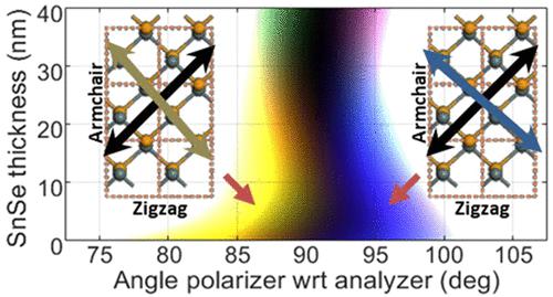
van der Waals (vdW) layered chalcogenides have strongly direction-dependent (i.e., anisotropic) properties that make them interesting for photonic and optoelectronic applications. Orthorhombic tin selenide (α-SnSe) is a triaxial vdW material with strong optical anisotropy within layer planes, which has motivated studies of optical phase and domain switching. As with every vdW material, controlling the orientation of crystal domains during growth is key to reliably making wafer-scale, high-quality thin films, free from twin boundaries. Here, we demonstrate a fast optical method to quantify domain orientation in SnSe thin films made by molecular beam epitaxy (MBE). The in-plane optical anisotropy results in white-light being reflected into distinct colors for certain optical polarization angles and the color depends on domain orientation. We use our method to confirm a high density of twin boundaries in SnSe epitaxial films on MgO substrates, with square symmetry that results in degeneracy between SnSe 90° domain orientations. We then demonstrate that growing on a-plane sapphire, with rectangular lattice-matched symmetry that breaks the SnSe domain degeneracy, results in single-crystalline films with one preferred orientation. Our SnSe bottom-up film synthesis by MBE enables future applications of this vdW material that is particularly difficult to process by top-down methods. Our optical metrology is fast and can apply to all triaxial vdW materials.
中文翻译:

使用快速光学计量和分子束外延测量并消除 SnSe 薄膜中的双畴
范德华 (vdW) 层状硫族化物具有强烈的方向依赖性(即各向异性)特性,这使得它们在光子和光电应用中很受关注。正交硒化锡 (α-SnSe) 是一种三轴 vdW 材料,在层平面内具有强光学各向异性,这激发了光学相位和畴切换的研究。与每一种 vdW 材料一样,在生长过程中控制晶畴的方向是可靠地制造晶圆级、高质量薄膜且没有双晶界的关键。在这里,我们展示了一种快速光学方法来量化由分子束外延 (MBE) 制成的 SnSe 薄膜中的畴取向。对于某些光学偏振角,面内光学各向异性导致白光被反射成不同的颜色,并且颜色取决于域方向。我们使用我们的方法来确认 MgO 衬底上的 SnSe 外延薄膜中的高密度孪晶边界,其正方形对称性导致 SnSe 90° 畴取向之间的退化。然后,我们证明在具有打破 SnSe 畴简并性的矩形晶格匹配对称性的 a 平面蓝宝石上生长,会产生具有一个优选取向的单晶薄膜。我们通过 MBE 进行的 SnSe 自下而上薄膜合成使这种 vdW 材料的未来应用成为可能,这种材料特别难以通过自上而下的方法进行处理。我们的光学计量速度很快,可以适用于所有三轴 vdW 材料。具有打破 SnSe 畴简并的矩形晶格匹配对称性,导致具有一个优选取向的单晶薄膜。我们通过 MBE 进行的 SnSe 自下而上薄膜合成使这种 vdW 材料的未来应用成为可能,这种材料特别难以通过自上而下的方法进行处理。我们的光学计量速度很快,可以适用于所有三轴 vdW 材料。具有打破 SnSe 畴简并的矩形晶格匹配对称性,导致具有一个优选取向的单晶薄膜。我们通过 MBE 进行的 SnSe 自下而上薄膜合成使这种 vdW 材料的未来应用成为可能,这种材料特别难以通过自上而下的方法进行处理。我们的光学计量速度很快,可以适用于所有三轴 vdW 材料。
更新日期:2022-06-16
中文翻译:
使用快速光学计量和分子束外延测量并消除 SnSe 薄膜中的双畴
范德华 (vdW) 层状硫族化物具有强烈的方向依赖性(即各向异性)特性,这使得它们在光子和光电应用中很受关注。正交硒化锡 (α-SnSe) 是一种三轴 vdW 材料,在层平面内具有强光学各向异性,这激发了光学相位和畴切换的研究。与每一种 vdW 材料一样,在生长过程中控制晶畴的方向是可靠地制造晶圆级、高质量薄膜且没有双晶界的关键。在这里,我们展示了一种快速光学方法来量化由分子束外延 (MBE) 制成的 SnSe 薄膜中的畴取向。对于某些光学偏振角,面内光学各向异性导致白光被反射成不同的颜色,并且颜色取决于域方向。我们使用我们的方法来确认 MgO 衬底上的 SnSe 外延薄膜中的高密度孪晶边界,其正方形对称性导致 SnSe 90° 畴取向之间的退化。然后,我们证明在具有打破 SnSe 畴简并性的矩形晶格匹配对称性的 a 平面蓝宝石上生长,会产生具有一个优选取向的单晶薄膜。我们通过 MBE 进行的 SnSe 自下而上薄膜合成使这种 vdW 材料的未来应用成为可能,这种材料特别难以通过自上而下的方法进行处理。我们的光学计量速度很快,可以适用于所有三轴 vdW 材料。具有打破 SnSe 畴简并的矩形晶格匹配对称性,导致具有一个优选取向的单晶薄膜。我们通过 MBE 进行的 SnSe 自下而上薄膜合成使这种 vdW 材料的未来应用成为可能,这种材料特别难以通过自上而下的方法进行处理。我们的光学计量速度很快,可以适用于所有三轴 vdW 材料。具有打破 SnSe 畴简并的矩形晶格匹配对称性,导致具有一个优选取向的单晶薄膜。我们通过 MBE 进行的 SnSe 自下而上薄膜合成使这种 vdW 材料的未来应用成为可能,这种材料特别难以通过自上而下的方法进行处理。我们的光学计量速度很快,可以适用于所有三轴 vdW 材料。


 京公网安备 11010802027423号