Our official English website, www.x-mol.net, welcomes your
feedback! (Note: you will need to create a separate account there.)
Engineering Graphene Grain Boundaries for Plasmonic Multi-Excitation and Hotspots
ACS Nano ( IF 15.8 ) Pub Date : 2022-06-13 , DOI: 10.1021/acsnano.2c00396 Teng Ma 1 , Baicheng Yao 2 , Zebo Zheng 3 , Zhibo Liu 1 , Wei Ma 1, 4 , Maolin Chen 1, 4 , Huanjun Chen 3 , Shaozhi Deng 3 , Ningsheng Xu 3 , Qiaoliang Bao 5, 6 , Dong-Ming Sun 1, 4 , Hui-Ming Cheng 1, 7 , Wencai Ren 1, 4
ACS Nano ( IF 15.8 ) Pub Date : 2022-06-13 , DOI: 10.1021/acsnano.2c00396 Teng Ma 1 , Baicheng Yao 2 , Zebo Zheng 3 , Zhibo Liu 1 , Wei Ma 1, 4 , Maolin Chen 1, 4 , Huanjun Chen 3 , Shaozhi Deng 3 , Ningsheng Xu 3 , Qiaoliang Bao 5, 6 , Dong-Ming Sun 1, 4 , Hui-Ming Cheng 1, 7 , Wencai Ren 1, 4
Affiliation
|
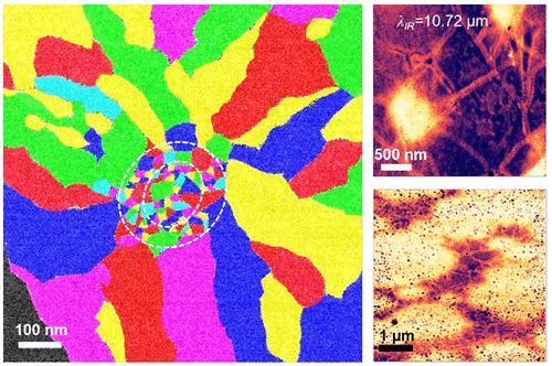
Surface plasmons, merging photonics and electronics in nanoscale dimensions, have been the cornerstones in integrated informatics, precision detection, high-resolution imaging, and energy conversion. Arising from the exceptional Fermi–Dirac tunability, ultrafast carrier mobility, and high-field confinement, graphene offers excellent advantages for plasmon technologies and enables a variety of state-of-the-art optoelectronic applications ranging from tight-field-enhanced light sources, modulators, and photodetectors to biochemical sensors. However, it is challenging to co-excite multiple graphene plasmons on one single graphene sheet with high density, a key step toward plasmonic wavelength-division multiplexing and next-generation dynamical optoelectronics. Here, we report the heteroepitaxial growth of a polycrystalline graphene monolayer with patterned gradient grain boundary density, which is synthesized by creating diverse nanosized local growth environments on a centimeter-scale substrate with a polycrystalline graphene ring seed in chemical vapor deposition. Such geometry enables plasmonic co-excitation with varied wavelength diversification in the nanoscale. Via using high-resolution scanning near-field optical microscopy, we demonstrate rich plasmon standing waves, even bright plasmonic hotspots with a size up to 3 μm. Moreover, by changing the grain boundary density and annealing, we find the local plasmonic wavelengths are widely tunable, from 70 to 300 nm. Theoretical modeling supports that such plasmonic versatility is due to the grain boundary-induced plasmon–phonon interactions through random phase approximation. The seed-induced heteroepitaxial growth provides a promising way for the grain boundary engineering of two-dimensional materials, and the controllable grain boundary-based plasmon co-generation and manipulation in one single graphene monolayer will facilitate the applications of graphene for plasmonics and nanophotonics.
中文翻译:

等离子体多激发和热点的工程石墨烯晶界
表面等离子体激元在纳米尺度上融合了光子学和电子学,已成为集成信息学、精密检测、高分辨率成像和能量转换的基石。源于卓越的费米-狄拉克可调谐性、超快载流子迁移率和高场限制,石墨烯为等离子体技术提供了卓越的优势,并使各种最先进的光电应用成为可能,从紧场增强光源,调制器和光电探测器到生化传感器。然而,在一张高密度石墨烯片上共激发多个石墨烯等离子体激元具有挑战性,这是实现等离子体波分复用和下一代动态光电子学的关键一步。这里,我们报告了具有图案化梯度晶界密度的多晶石墨烯单层的异质外延生长,这是通过在化学气相沉积中使用多晶石墨烯环晶种在厘米级衬底上创建不同的纳米级局部生长环境合成的。这种几何形状使等离子体共激发与纳米级的不同波长多样化成为可能。通过使用高分辨率扫描近场光学显微镜,我们展示了丰富的等离子体激元驻波,甚至是尺寸高达 3 μm 的明亮等离子体激元热点。此外,通过改变晶界密度和退火,我们发现局域等离子体波长在 70 到 300 nm 范围内可调。理论模型支持这种等离子体的多功能性是由于晶界通过随机相位近似引起的等离子体 - 声子相互作用。种子诱导的异质外延生长为二维材料的晶界工程提供了一种有前途的方法,并且在单个石墨烯单层中基于晶界的可控等离子体共生和操纵将促进石墨烯在等离子体和纳米光子学中的应用。
更新日期:2022-06-13
中文翻译:
等离子体多激发和热点的工程石墨烯晶界
表面等离子体激元在纳米尺度上融合了光子学和电子学,已成为集成信息学、精密检测、高分辨率成像和能量转换的基石。源于卓越的费米-狄拉克可调谐性、超快载流子迁移率和高场限制,石墨烯为等离子体技术提供了卓越的优势,并使各种最先进的光电应用成为可能,从紧场增强光源,调制器和光电探测器到生化传感器。然而,在一张高密度石墨烯片上共激发多个石墨烯等离子体激元具有挑战性,这是实现等离子体波分复用和下一代动态光电子学的关键一步。这里,我们报告了具有图案化梯度晶界密度的多晶石墨烯单层的异质外延生长,这是通过在化学气相沉积中使用多晶石墨烯环晶种在厘米级衬底上创建不同的纳米级局部生长环境合成的。这种几何形状使等离子体共激发与纳米级的不同波长多样化成为可能。通过使用高分辨率扫描近场光学显微镜,我们展示了丰富的等离子体激元驻波,甚至是尺寸高达 3 μm 的明亮等离子体激元热点。此外,通过改变晶界密度和退火,我们发现局域等离子体波长在 70 到 300 nm 范围内可调。理论模型支持这种等离子体的多功能性是由于晶界通过随机相位近似引起的等离子体 - 声子相互作用。种子诱导的异质外延生长为二维材料的晶界工程提供了一种有前途的方法,并且在单个石墨烯单层中基于晶界的可控等离子体共生和操纵将促进石墨烯在等离子体和纳米光子学中的应用。


 京公网安备 11010802027423号