Our official English website, www.x-mol.net, welcomes your
feedback! (Note: you will need to create a separate account there.)
Probing the Efficacy of Large-Scale Nonporous IGZO for Visible-to-NIR Detection Capability: An Approach toward High-Performance Image Sensor Circuitry
ACS Nano ( IF 15.8 ) Pub Date : 2022-06-13 , DOI: 10.1021/acsnano.2c01773 Anamika Sen 1 , Heekyeong Park 2 , Pavan Pujar 1 , Arindam Bala 1 , Haewon Cho 1 , Na Liu 1 , Srinivas Gandla 1 , Sunkook Kim 1
ACS Nano ( IF 15.8 ) Pub Date : 2022-06-13 , DOI: 10.1021/acsnano.2c01773 Anamika Sen 1 , Heekyeong Park 2 , Pavan Pujar 1 , Arindam Bala 1 , Haewon Cho 1 , Na Liu 1 , Srinivas Gandla 1 , Sunkook Kim 1
Affiliation
|
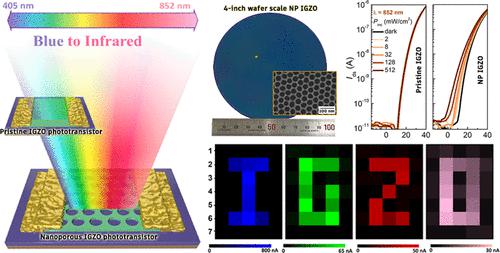
The technological ability to detect a wide spectrum range of illuminated visible-to-NIR is substantially improved for an amorphous metal oxide semiconductor, indium gallium zinc oxide (IGZO), without employing an additional photoabsorber. The fundamentally tuned morphology via structural engineering results in the creation of nanopores throughout the entire thickness of ∼30 nm. See-through nanopores have edge functionalization with vacancies, which leads to a large density of substates near the conduction band minima and valence band maxima. The presence of nanoring edges with a high concentration of vacancies is investigated using chemical composition analysis. The process of creating a nonporous morphology is sophisticated and is demonstrated using a wafer-scale phototransistor array. The performance of the phototransistors is assessed in terms of photosensitivity (S) and photoresponsivity (R); both are of high magnitudes (S = 8.6 × 10⁴ at λex = 638 nm and Pinc = 512 mW cm2–; R = 120 A W1– at Pinc = 2 mW cm2– for the same λex). Additionally, the 7 × 5 array of 35 phototransistors is effective in sensing and reproducing the input image by responding to selectively illuminated pixels.
中文翻译:

探索大规模无孔 IGZO 对可见光到近红外检测能力的功效:一种实现高性能图像传感器电路的方法
在不使用额外的光吸收剂的情况下,非晶金属氧化物半导体、氧化铟镓锌 (IGZO) 检测宽光谱范围的可见光到近红外光的技术能力得到了显着提高。通过结构工程从根本上调整的形态导致在约 30 nm 的整个厚度中产生纳米孔。透明纳米孔具有带空位的边缘功能化,这导致导带最小值和价带最大值附近的大密度子态。使用化学成分分析研究了具有高浓度空位的纳米环边缘的存在。创建无孔形态的过程非常复杂,并使用晶圆级光电晶体管阵列进行了演示。S ) 和光响应性 ( R ); 两者的震级都很高(S = 8.6 × 10 4在 λ ex = 638 nm 和P inc = 512 mW cm 2–;R = 120 AW 1–在P inc = 2 mW cm 2–对于相同的 λ ex)。此外,由 35 个光电晶体管组成的 7 × 5 阵列可通过响应选择性照明像素来有效感测和再现输入图像。
更新日期:2022-06-13
中文翻译:
探索大规模无孔 IGZO 对可见光到近红外检测能力的功效:一种实现高性能图像传感器电路的方法
在不使用额外的光吸收剂的情况下,非晶金属氧化物半导体、氧化铟镓锌 (IGZO) 检测宽光谱范围的可见光到近红外光的技术能力得到了显着提高。通过结构工程从根本上调整的形态导致在约 30 nm 的整个厚度中产生纳米孔。透明纳米孔具有带空位的边缘功能化,这导致导带最小值和价带最大值附近的大密度子态。使用化学成分分析研究了具有高浓度空位的纳米环边缘的存在。创建无孔形态的过程非常复杂,并使用晶圆级光电晶体管阵列进行了演示。S ) 和光响应性 ( R ); 两者的震级都很高(S = 8.6 × 10 4在 λ ex = 638 nm 和P inc = 512 mW cm 2–;R = 120 AW 1–在P inc = 2 mW cm 2–对于相同的 λ ex)。此外,由 35 个光电晶体管组成的 7 × 5 阵列可通过响应选择性照明像素来有效感测和再现输入图像。


 京公网安备 11010802027423号