Journal of Alloys and Compounds ( IF 6.2 ) Pub Date : 2022-05-19 , DOI: 10.1016/j.jallcom.2022.165429 Tian Tian , Xiaohui Song , Zhen Liu , Zinan Ma , Baomei Wang , Bingrui Wang , Xueping Li , Yong Yan , Yurong Jiang , Shuyi Wei , Congxin Xia
|
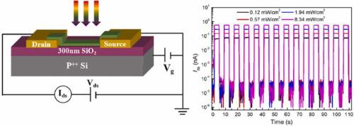
Recently, BiI3 was discovered as a promising 2D semiconductor materials for photovoltaic and photodetector device, due to its suitable bandgap, high optical absorption coefficient, excellent electron mobility, and low carrier concentration. However, as so far, only the CVD/PVD grown BiI3 nanoflakes/films have been reported. Here, we firstly synthesized the O-doped BiI3 (OBI) bulk crystals via chemical vapor transport (CVT) method, and then systematically studied the electrical and optoelectronic properties of exfoliated multi-layer OBI nanoflakes. Back-gated field-effect transistor fabricated on the multi-layer OBI nanoflakes with van der Waals (vdW) bottom electrode contact exhibited n-type semiconducting characteristics. In addition, exfoliated multi-layer OBI based photodetector demonstrates an excellent photoresponse with good reproducibility at room-temperature for visible wavelengths, including a high photo-to-dark current ratio (2.16 ×10⁴), a remarkable photoresponsivity (850 mA W−1), a fast response speed (rise/decay time of 3.2/2.9 ms), and a high specific detectivity (9.85 ×10¹² Jones), which is favored by the ultralow dark current (∼30 fA). These results indicated that the OBI crystals have great potential for future applications in highly sensitive and ultrafast visible-light photodetector.
中文翻译:
基于多层O掺杂BiI3纳米薄片的超高灵敏度可见光光电探测器
最近,BiI 3因其合适的带隙、高光吸收系数、优异的电子迁移率和低载流子浓度而被认为是一种有前途的用于光伏和光电探测器器件的二维半导体材料。然而,到目前为止,仅报道了CVD/PVD生长的BiI 3纳米薄片/薄膜。在这里,我们首先合成了O掺杂的BiI 3(OBI) 通过化学气相传输 (CVT) 方法制备块状晶体,然后系统地研究了剥离的多层 OBI 纳米薄片的电学和光电特性。在具有范德华 (vdW) 底部电极接触的多层 OBI 纳米薄片上制造的背栅场效应晶体管表现出 n 型半导体特性。此外,剥离的多层 OBI 光电探测器在室温下对可见光波长表现出优异的光响应和良好的再现性,包括高光暗电流比 (2.16 ×10 4 )、显着的光响应 (850 mA W - 1),响应速度快(上升/衰减时间为3.2/2.9 ms),比检测率高(9.85×10 12Jones),它受到超低暗电流(~30 fA)的青睐。这些结果表明,OBI晶体在高灵敏度和超快可见光光电探测器中具有巨大的应用潜力。


 京公网安备 11010802027423号