当前位置:
X-MOL 学术
›
Chem. Soc. Rev.
›
论文详情
Our official English website, www.x-mol.net, welcomes your
feedback! (Note: you will need to create a separate account there.)
Lateral layered semiconductor multijunctions for novel electronic devices
Chemical Society Reviews ( IF 40.4 ) Pub Date : 2022-04-28 , DOI: 10.1039/d1cs01092a Simian Zhang 1 , Xiaonan Deng 1 , Yifei Wu 1 , Yuqi Wang 1 , Shengxian Ke 1 , Shishu Zhang 2 , Kai Liu 1 , Ruitao Lv 1 , Zhengcao Li 1 , Qihua Xiong 2, 3, 4 , Chen Wang 1
Chemical Society Reviews ( IF 40.4 ) Pub Date : 2022-04-28 , DOI: 10.1039/d1cs01092a Simian Zhang 1 , Xiaonan Deng 1 , Yifei Wu 1 , Yuqi Wang 1 , Shengxian Ke 1 , Shishu Zhang 2 , Kai Liu 1 , Ruitao Lv 1 , Zhengcao Li 1 , Qihua Xiong 2, 3, 4 , Chen Wang 1
Affiliation
|
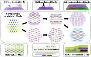
Layered semiconductors, represented by transition metal dichalcogenides, have attached extensive attention due to their unique and tunable electrical and optical properties. In particular, lateral layered semiconductor multijunctions, including homojunctions, heterojunctions, hybrid junctions and superlattices, present a totally new degree of freedom in research on electronic devices beyond traditional materials and their structures, providing unique opportunities for the development of new structures and operation principle-based high performance devices. However, the advances in this field are limited by the precise synthesis of high-quality junctions and greatly hampered by ambiguous device performance limits. Herein, we review the recent key breakthroughs in the design, synthesis, electronic structure and property modulation of lateral semiconductor multijunctions and focus on their application-specific devices. Specifically, the synthesis methods based on different principles, such as chemical and external source-induced methods, are introduced stepwise for the controllable fabrication of semiconductor multijunctions as the basics of device application. Subsequently, their structure and property modulation are discussed, including control of their electronic structure, exciton dynamics and optical properties before the fabrication of lateral layered semiconductor multijunction devices. Precise property control will potentially result in outstanding device performances, including high-quality diodes and FETs, scalable logic and analog circuits, highly efficient optoelectronic devices, and unique electrochemical devices. Lastly, we focus on several of the most essential but unresolved debates in this field, such as the true advantages of few-layer vs. monolayer multijunctions, how sharp the interface should be for specific functional devices, and the superiority of lateral multijunctions over vertical multijunctions, highlighting the next-phase strategy to enhance the performance potential of lateral multijunction devices.
中文翻译:

用于新型电子器件的横向层状半导体多结
以过渡金属二硫属化物为代表的层状半导体由于其独特且可调谐的电学和光学特性而受到广泛关注。特别是横向层状半导体多结,包括同质结、异质结、混合结和超晶格,为电子器件的研究提供了超越传统材料及其结构的全新自由度,为开发新结构和工作原理提供了独特的机会——基于高性能设备。然而,该领域的进展受到高质量结的精确合成的限制,并且受到模棱两可的器件性能限制的极大阻碍。在此,我们回顾了近期在设计、合成、横向半导体多结的电子结构和特性调制,并专注于其专用器件。具体而言,逐步介绍了基于不同原理的合成方法,例如化学和外部源诱导方法,用于半导体多结的可控制造,作为器件应用的基础。随后,讨论了它们的结构和特性调制,包括在制造横向层状半导体多结器件之前对其电子结构、激子动力学和光学特性的控制。精确的属性控制可能会带来出色的器件性能,包括高质量的二极管和 FET、可扩展的逻辑和模拟电路、高效的光电器件和独特的电化学器件。与单层多结相比,特定功能器件的界面应该有多锐利,以及横向多结相对于垂直多结的优越性,突出了提高横向多结器件性能潜力的下一阶段策略。
更新日期:2022-04-28
中文翻译:
用于新型电子器件的横向层状半导体多结
以过渡金属二硫属化物为代表的层状半导体由于其独特且可调谐的电学和光学特性而受到广泛关注。特别是横向层状半导体多结,包括同质结、异质结、混合结和超晶格,为电子器件的研究提供了超越传统材料及其结构的全新自由度,为开发新结构和工作原理提供了独特的机会——基于高性能设备。然而,该领域的进展受到高质量结的精确合成的限制,并且受到模棱两可的器件性能限制的极大阻碍。在此,我们回顾了近期在设计、合成、横向半导体多结的电子结构和特性调制,并专注于其专用器件。具体而言,逐步介绍了基于不同原理的合成方法,例如化学和外部源诱导方法,用于半导体多结的可控制造,作为器件应用的基础。随后,讨论了它们的结构和特性调制,包括在制造横向层状半导体多结器件之前对其电子结构、激子动力学和光学特性的控制。精确的属性控制可能会带来出色的器件性能,包括高质量的二极管和 FET、可扩展的逻辑和模拟电路、高效的光电器件和独特的电化学器件。与单层多结相比,特定功能器件的界面应该有多锐利,以及横向多结相对于垂直多结的优越性,突出了提高横向多结器件性能潜力的下一阶段策略。


 京公网安备 11010802027423号