当前位置:
X-MOL 学术
›
Acc. Mater. Res.
›
论文详情
Our official English website, www.x-mol.net, welcomes your
feedback! (Note: you will need to create a separate account there.)
Low-Dose Electron Microscopy Imaging of Electron Beam-Sensitive Crystalline Materials
Accounts of Materials Research ( IF 14.0 ) Pub Date : 2022-04-19 , DOI: 10.1021/accountsmr.2c00008 Jia Lv 1 , Hui Zhang 2 , Daliang Zhang 1 , Lingmei Liu 1 , Yu Han 2
Accounts of Materials Research ( IF 14.0 ) Pub Date : 2022-04-19 , DOI: 10.1021/accountsmr.2c00008 Jia Lv 1 , Hui Zhang 2 , Daliang Zhang 1 , Lingmei Liu 1 , Yu Han 2
Affiliation
|
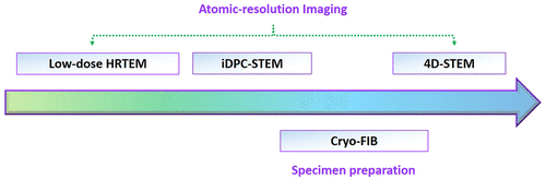
As one of the most widely used characterization tools in materials science, (scanning) transmission electron microscopy ((S)TEM) has the unique ability to directly image specimens with atomic resolution. Compared to diffraction-based techniques, the main advantage of (S)TEM imaging is that in addition to the periodic average structures of crystalline materials, it can be used to probe nonperiodic local structures such as surfaces, interfaces, dopants, and defects, which have crucial impacts on material properties. However, many crystalline materials are extremely sensitive to electron beam irradiation, which can only withstand dozens (or even fewer) of electrons per square angstrom before they undergo structural damage. Although using electron doses lower than the thresholds can in principle preserve their structures, the thus acquired images are too noisy to be useful. Consequently, high-resolution imaging of the inherent structures of such electron beam-sensitive materials using (S)TEM is a long-standing challenge. In recent years, the advances in electron detectors and image-acquisition methods have enabled high-resolution (S)TEM with ultralow electron doses, largely overcoming this challenge. A series of highly electron beam-sensitive materials that are traditionally considered impossible to be imaged with (S)TEM, including metal organic frameworks (MOFs), covalent organic frameworks (COFs), organic–inorganic hybrid halide perovskites, and supramolecular crystals, have been successfully imaged at atomic resolutions. This technological advance has greatly expanded the application range of electron microscopy.
中文翻译:

电子束敏感晶体材料的低剂量电子显微镜成像
作为材料科学中使用最广泛的表征工具之一,(扫描)透射电子显微镜((S)TEM)具有以原子分辨率直接成像样品的独特能力。与基于衍射的技术相比,(S)TEM 成像的主要优势在于,除了晶体材料的周期性平均结构外,它还可以用于探测表面、界面、掺杂剂和缺陷等非周期性局部结构,这对材料性能有重要影响。然而,许多晶体材料对电子束辐照极为敏感,每平方埃只能承受几十个(甚至更少)的电子,然后才会发生结构损伤。虽然使用低于阈值的电子剂量原则上可以保留它们的结构,这样获得的图像噪声太大而无用。因此,使用 (S)TEM 对此类电子束敏感材料的固有结构进行高分辨率成像是一项长期挑战。近年来,电子探测器和图像采集方法的进步使得具有超低电子剂量的高分辨率 (S)TEM 成为可能,在很大程度上克服了这一挑战。一系列传统上认为不可能用 (S)TEM 成像的高电子束敏感材料,包括金属有机骨架 (MOF)、共价有机骨架 (COF)、有机-无机杂化卤化物钙钛矿和超分子晶体,以原子分辨率成功成像。这一技术进步极大地扩展了电子显微镜的应用范围。使用 (S)TEM 对这种电子束敏感材料的固有结构进行高分辨率成像是一项长期挑战。近年来,电子探测器和图像采集方法的进步使得具有超低电子剂量的高分辨率 (S)TEM 成为可能,在很大程度上克服了这一挑战。一系列传统上认为不可能用 (S)TEM 成像的高电子束敏感材料,包括金属有机骨架 (MOF)、共价有机骨架 (COF)、有机-无机杂化卤化物钙钛矿和超分子晶体,以原子分辨率成功成像。这一技术进步极大地扩展了电子显微镜的应用范围。使用 (S)TEM 对这种电子束敏感材料的固有结构进行高分辨率成像是一项长期挑战。近年来,电子探测器和图像采集方法的进步使得具有超低电子剂量的高分辨率 (S)TEM 成为可能,在很大程度上克服了这一挑战。一系列传统上认为不可能用 (S)TEM 成像的高电子束敏感材料,包括金属有机骨架 (MOF)、共价有机骨架 (COF)、有机-无机杂化卤化物钙钛矿和超分子晶体,以原子分辨率成功成像。这一技术进步极大地扩展了电子显微镜的应用范围。
更新日期:2022-04-19
中文翻译:
电子束敏感晶体材料的低剂量电子显微镜成像
作为材料科学中使用最广泛的表征工具之一,(扫描)透射电子显微镜((S)TEM)具有以原子分辨率直接成像样品的独特能力。与基于衍射的技术相比,(S)TEM 成像的主要优势在于,除了晶体材料的周期性平均结构外,它还可以用于探测表面、界面、掺杂剂和缺陷等非周期性局部结构,这对材料性能有重要影响。然而,许多晶体材料对电子束辐照极为敏感,每平方埃只能承受几十个(甚至更少)的电子,然后才会发生结构损伤。虽然使用低于阈值的电子剂量原则上可以保留它们的结构,这样获得的图像噪声太大而无用。因此,使用 (S)TEM 对此类电子束敏感材料的固有结构进行高分辨率成像是一项长期挑战。近年来,电子探测器和图像采集方法的进步使得具有超低电子剂量的高分辨率 (S)TEM 成为可能,在很大程度上克服了这一挑战。一系列传统上认为不可能用 (S)TEM 成像的高电子束敏感材料,包括金属有机骨架 (MOF)、共价有机骨架 (COF)、有机-无机杂化卤化物钙钛矿和超分子晶体,以原子分辨率成功成像。这一技术进步极大地扩展了电子显微镜的应用范围。使用 (S)TEM 对这种电子束敏感材料的固有结构进行高分辨率成像是一项长期挑战。近年来,电子探测器和图像采集方法的进步使得具有超低电子剂量的高分辨率 (S)TEM 成为可能,在很大程度上克服了这一挑战。一系列传统上认为不可能用 (S)TEM 成像的高电子束敏感材料,包括金属有机骨架 (MOF)、共价有机骨架 (COF)、有机-无机杂化卤化物钙钛矿和超分子晶体,以原子分辨率成功成像。这一技术进步极大地扩展了电子显微镜的应用范围。使用 (S)TEM 对这种电子束敏感材料的固有结构进行高分辨率成像是一项长期挑战。近年来,电子探测器和图像采集方法的进步使得具有超低电子剂量的高分辨率 (S)TEM 成为可能,在很大程度上克服了这一挑战。一系列传统上认为不可能用 (S)TEM 成像的高电子束敏感材料,包括金属有机骨架 (MOF)、共价有机骨架 (COF)、有机-无机杂化卤化物钙钛矿和超分子晶体,以原子分辨率成功成像。这一技术进步极大地扩展了电子显微镜的应用范围。


 京公网安备 11010802027423号