Applied Surface Science ( IF 6.3 ) Pub Date : 2022-01-13 , DOI: 10.1016/j.apsusc.2021.152373 Nobuyuki Ishida 1 , Takaaki Mano 1 , Takeshi Noda 1
|
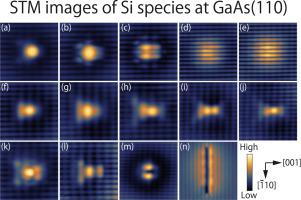
Characterizing the atomic arrangement and distribution of dopant atoms is important for the fundamental understanding of the effects of doping on the electronic properties of semiconductors. Here, we used scanning tunneling microscopy (STM) to image the dopant species in highly Si-doped GaAs. Based on the distinct features in the STM images, we identified the most common Si species, which enabled the accurate evaluation of the local donor and acceptor concentrations and their in-plane variation across different regions. Systematic analysis of the variation of these properties with the doping concentration and the changes after the post-annealing process allowed atomic-scale information about the detailed behaviors of the Si species to be directly extracted. Our findings provided strong insights into the possible roles of each Si species in modifying the macroscopic electronic properties of GaAs.
中文翻译:
使用扫描隧道显微镜对 GaAs 中高掺杂 Si 杂质的原子尺度表征
表征掺杂原子的原子排列和分布对于从根本上理解掺杂对半导体电子特性的影响非常重要。在这里,我们使用扫描隧道显微镜 (STM) 对高度 Si 掺杂的 GaAs 中的掺杂剂种类进行成像。基于 STM 图像中的不同特征,我们确定了最常见的 Si 物种,从而能够准确评估局部供体和受体浓度及其在不同区域的平面内变化。系统分析这些性质随掺杂浓度的变化以及后退火工艺后的变化,可以直接提取有关 Si 物种详细行为的原子级信息。


 京公网安备 11010802027423号