当前位置:
X-MOL 学术
›
Adv. Funct. Mater.
›
论文详情
Our official English website, www.x-mol.net, welcomes your
feedback! (Note: you will need to create a separate account there.)
Patterning All-Inorganic Halide Perovskite with Adjustable Phase for High-Resolution Color Filter and Photodetector Arrays
Advanced Functional Materials ( IF 18.5 ) Pub Date : 2022-01-03 , DOI: 10.1002/adfm.202111409 Woosik Kim 1 , Su‐Kyung Kim 1 , Sanghyun Jeon 1 , Junhyuk Ahn 1 , Byung Ku Jung 1 , Sang Yeop Lee 1 , Chanho Shin 2 , Tae‐Yeon Seong 1 , Sohee Jeong 3 , Ho Seong Jang 3 , TSe Nga Ng 2 , Soong Ju Oh 1
Advanced Functional Materials ( IF 18.5 ) Pub Date : 2022-01-03 , DOI: 10.1002/adfm.202111409 Woosik Kim 1 , Su‐Kyung Kim 1 , Sanghyun Jeon 1 , Junhyuk Ahn 1 , Byung Ku Jung 1 , Sang Yeop Lee 1 , Chanho Shin 2 , Tae‐Yeon Seong 1 , Sohee Jeong 3 , Ho Seong Jang 3 , TSe Nga Ng 2 , Soong Ju Oh 1
Affiliation
|
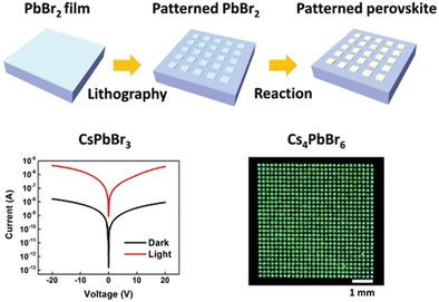
Perovskite has been actively studied for optoelectronic applications, such as photodetectors and light-emitting diodes (LEDs), because of its excellent optoelectronic properties. However, ionic bonds of the perovskite structure are vulnerable to chemicals, which makes perovskite incompatible with photolithography processes that use polar solvents. Such incompatibility with photolithography hinders perovskite patterning and device integration. Here, an all-solution based cesium lead halide perovskite (CsxPbyBrz) patterning method is introduced in which PbBr2 is patterned and then synthesized into CsxPbyBrz. Each step of the top-down patterning process (e.g., developing, etching, and rinsing) is designed to be compatible with existing photolithography equipment. Structural, chemical, and optical analyses show that the PbBr2 pattern of (10 µm)2 squares is successfully transformed into CsPbBr3 and Cs4PbBr6 with excellent absorption and emission properties. High-resolution photoconductor arrays and luminescent pattern arrays are fabricated with CsPbBr3 and Cs4PbBr6 on various substrates, including flexible plastic films, to demonstrate their potential applications in image sensors or displays. The research provides a fundamental understanding of the properties and growth of perovskite and promotes technological advancement by preventing degradation during the photolithography process, enabling the integration of perovskite arrays into image sensors and displays.
中文翻译:

用于高分辨率彩色滤光片和光电探测器阵列的可调节相位全无机卤化物钙钛矿图案化
钙钛矿因其优异的光电特性而被积极研究用于光电应用,例如光电探测器和发光二极管 (LED)。然而,钙钛矿结构的离子键容易受到化学物质的影响,这使得钙钛矿与使用极性溶剂的光刻工艺不兼容。这种与光刻的不相容性阻碍了钙钛矿图案化和器件集成。本文介绍了一种基于全溶液的铯铅卤化钙钛矿 (Cs x Pb y Br z ) 图案化方法,其中 PbBr 2被图案化,然后合成为 Cs x Pb y Br z. 自上而下的图案化工艺(例如,显影、蚀刻和冲洗)的每个步骤都设计为与现有的光刻设备兼容。结构、化学和光学分析表明,(10 µm) 2正方形的PbBr 2图案成功地转化为具有优异吸收和发射特性的CsPbBr 3和Cs 4 PbBr 6 。使用 CsPbBr 3和 Cs 4 PbBr 6制造高分辨率光电导体阵列和发光图案阵列在包括柔性塑料薄膜在内的各种基材上,以展示它们在图像传感器或显示器中的潜在应用。该研究提供了对钙钛矿特性和生长的基本理解,并通过防止光刻过程中的降解来促进技术进步,从而将钙钛矿阵列集成到图像传感器和显示器中。
更新日期:2022-01-03
中文翻译:
用于高分辨率彩色滤光片和光电探测器阵列的可调节相位全无机卤化物钙钛矿图案化
钙钛矿因其优异的光电特性而被积极研究用于光电应用,例如光电探测器和发光二极管 (LED)。然而,钙钛矿结构的离子键容易受到化学物质的影响,这使得钙钛矿与使用极性溶剂的光刻工艺不兼容。这种与光刻的不相容性阻碍了钙钛矿图案化和器件集成。本文介绍了一种基于全溶液的铯铅卤化钙钛矿 (Cs x Pb y Br z ) 图案化方法,其中 PbBr 2被图案化,然后合成为 Cs x Pb y Br z. 自上而下的图案化工艺(例如,显影、蚀刻和冲洗)的每个步骤都设计为与现有的光刻设备兼容。结构、化学和光学分析表明,(10 µm) 2正方形的PbBr 2图案成功地转化为具有优异吸收和发射特性的CsPbBr 3和Cs 4 PbBr 6 。使用 CsPbBr 3和 Cs 4 PbBr 6制造高分辨率光电导体阵列和发光图案阵列在包括柔性塑料薄膜在内的各种基材上,以展示它们在图像传感器或显示器中的潜在应用。该研究提供了对钙钛矿特性和生长的基本理解,并通过防止光刻过程中的降解来促进技术进步,从而将钙钛矿阵列集成到图像传感器和显示器中。


 京公网安备 11010802027423号