当前位置:
X-MOL 学术
›
Acc. Chem. Res.
›
论文详情
Our official English website, www.x-mol.net, welcomes your feedback! (Note: you will need to create a separate account there.)
Traversing Excitonic and Ionic Landscapes: Reduced-Dimensionality-Inspired Design of Organometal Halide Semiconductors for Energy Applications
Accounts of Chemical Research ( IF 18.3 ) Pub Date : 2021-11-29 , DOI: 10.1021/acs.accounts.1c00492 Daniel Powell 1 , Kameron R Hansen 1 , Laura Flannery 1 , Luisa Whittaker-Brooks 1
Accounts of Chemical Research ( IF 18.3 ) Pub Date : 2021-11-29 , DOI: 10.1021/acs.accounts.1c00492 Daniel Powell 1 , Kameron R Hansen 1 , Laura Flannery 1 , Luisa Whittaker-Brooks 1
Affiliation
|
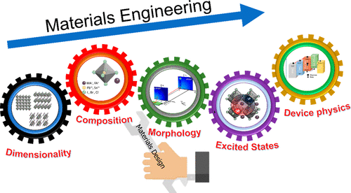
At the very heart of the global semiconductor industry lies the omnipresent push for new materials discovery. New materials constantly rise and fall out of fashion in the scientific literature, with those passing an initial phase of research scrutiny becoming hotbeds of characterization and optimization efforts. Yet, innumerable hours of painstaking research have been devoted to materials that have ultimately fallen by the wayside after crossing over an indefinable threshold, whereupon historical optimism is met with newfound skepticism. Materials have to perform well, and they have to do it quickly. In the past decade, metal-halide perovskites (MHPs) have garnered widespread attention. The hegemonic view in both academic and industrial circles is that these materials could be engineered to meet the demands of the semiconductor industry. Their promise as inexpensive solar cell devices is highly attractive, and it has been nothing short of remarkable that efficiencies have risen from 3.8% in 2009 to more than 25.5% in 2021. Moreover, MHPs are poised to be revolutionary materials in more ways than one. The highest MHP LED efficiency was recently reported (23.4%), and MHPs have demonstrated promise in photodetectors, memristors, and transistors. However, the many excellent properties of MHPs are contrasted by longstanding stability and reproducibility limitations that have hindered their commercialization. Overcoming the limitations of MHPs is ultimately a materials engineering problem, which should be solved by mapping more precise relationships between structure, composition, and device performance. In 1958, Francis Crick famously developed the central dogma of molecular biology which describes the unidirectional flow of information in biological systems. In the words of Crick, “nature has devised a unique instrument in which an underlying simplicity is used to express great subtlety and versatility.” In this Account, taking inspiration from the hierarchical organization of nature, we describe a hierarchical approach to materials engineering of organic metal-halide semiconductors. We demonstrate that organo-metal halide semiconductors’ dimensionality, composition, and morphology dictate their optoelectronic properties and can be exploited in defining more explicit relationships between structure and function. Here, we traverse three-dimensional (3D), two-dimensional (2D), and one-dimensional (1D) organo-metal halide semiconductors, detailing the morphological and compositional differences in each and the implications that can be drawn within each domain on the engineering process. Control over ion migration pathways via morphology engineering as well as control over charge formation in organic–inorganic semiconductors is demonstrated. Fundamental insights into the amount of static and dynamic disorder in the MHP lattice are provided, which can be continuously tuned as a function of composition and morphology. Using electroabsorption spectroscopy on 2D MHPs, a disorder-induced dipole moment in the exciton proportional to the summed value of static and dynamic disorder is measured. Spectroscopic isolation of exciton features in 2D MHP electroabsorption spectra allows us to obtain precise, model-independent measurements of exciton binding energies to study the effect of chemical substitutions, such as Sn2+ → Pb2+, on the value of the exciton binding energy. Finally, we conclude that this multidimensional platform, with the aid of machine learning and robotics, will be foundational in accurately predicting structure–property–device relationships in organo-metal halide semiconductors in the future.
中文翻译:

穿越激子和离子景观:用于能源应用的有机金属卤化物半导体的降维设计
全球半导体行业的核心是对新材料发现的无所不在的推动。新材料在科学文献中不断兴衰,那些通过研究审查的初始阶段成为表征和优化工作的温床。然而,无数小时的艰苦研究一直致力于研究在跨越一个无法定义的门槛后最终被抛在一边的材料,因此历史的乐观主义遭到了新发现的怀疑主义。材料必须表现良好,而且必须快速完成。在过去的十年中,金属卤化物钙钛矿(MHPs)引起了广泛的关注。学术界和工业界的霸权观点是,这些材料可以被设计来满足半导体行业的需求。它们作为廉价太阳能电池设备的承诺极具吸引力,其效率从 2009 年的 3.8% 提高到 2021 年的 25.5% 以上,这一点非常引人注目。此外,MHP 有望在不止一个方面成为革命性材料. 最近报道了最高的 MHP LED 效率 (23.4%),并且 MHP 在光电探测器、忆阻器和晶体管中已显示出前景。然而,MHP 的许多优良特性与阻碍其商业化的长期稳定性和可重复性限制形成鲜明对比。克服 MHP 的局限性最终是一个材料工程问题,应该通过映射结构、成分和器件性能之间更精确的关系来解决。1958 年,弗朗西斯·克里克 (Francis Crick) 提出了著名的分子生物学中心法则,该法则描述了生物系统中信息的单向流动。用克里克的话来说,“大自然设计了一种独特的工具,其中潜在的简单性被用来表达巨大的微妙性和多功能性。” 在这个帐户中,从自然界的分层组织中汲取灵感,我们描述了有机金属卤化物半导体材料工程的分层方法。我们证明了有机金属卤化物半导体的维度、组成和形态决定了它们的光电特性,并且可以用于定义结构和功能之间更明确的关系。在这里,我们遍历了三维 (3D)、二维 (2D) 和一维 (1D) 有机金属卤化物半导体,详细说明每个领域的形态和成分差异,以及每个领域对工程过程的影响。证明了通过形态工程控制离子迁移路径以及控制有机-无机半导体中的电荷形成。提供了对 MHP 晶格中静态和动态无序数量的基本见解,可以根据成分和形态连续调整。使用二维 MHP 上的电吸收光谱,测量激子中与静态和动态无序的总和值成比例的无序诱导偶极矩。二维 MHP 电吸收光谱中激子特征的光谱分离使我们能够获得精确的、2+ → Pb 2+,关于激子结合能的值。最后,我们得出结论,在机器学习和机器人技术的帮助下,这个多维平台将成为未来准确预测有机金属卤化物半导体结构-性能-器件关系的基础。
更新日期:2021-12-07
中文翻译:
穿越激子和离子景观:用于能源应用的有机金属卤化物半导体的降维设计
全球半导体行业的核心是对新材料发现的无所不在的推动。新材料在科学文献中不断兴衰,那些通过研究审查的初始阶段成为表征和优化工作的温床。然而,无数小时的艰苦研究一直致力于研究在跨越一个无法定义的门槛后最终被抛在一边的材料,因此历史的乐观主义遭到了新发现的怀疑主义。材料必须表现良好,而且必须快速完成。在过去的十年中,金属卤化物钙钛矿(MHPs)引起了广泛的关注。学术界和工业界的霸权观点是,这些材料可以被设计来满足半导体行业的需求。它们作为廉价太阳能电池设备的承诺极具吸引力,其效率从 2009 年的 3.8% 提高到 2021 年的 25.5% 以上,这一点非常引人注目。此外,MHP 有望在不止一个方面成为革命性材料. 最近报道了最高的 MHP LED 效率 (23.4%),并且 MHP 在光电探测器、忆阻器和晶体管中已显示出前景。然而,MHP 的许多优良特性与阻碍其商业化的长期稳定性和可重复性限制形成鲜明对比。克服 MHP 的局限性最终是一个材料工程问题,应该通过映射结构、成分和器件性能之间更精确的关系来解决。1958 年,弗朗西斯·克里克 (Francis Crick) 提出了著名的分子生物学中心法则,该法则描述了生物系统中信息的单向流动。用克里克的话来说,“大自然设计了一种独特的工具,其中潜在的简单性被用来表达巨大的微妙性和多功能性。” 在这个帐户中,从自然界的分层组织中汲取灵感,我们描述了有机金属卤化物半导体材料工程的分层方法。我们证明了有机金属卤化物半导体的维度、组成和形态决定了它们的光电特性,并且可以用于定义结构和功能之间更明确的关系。在这里,我们遍历了三维 (3D)、二维 (2D) 和一维 (1D) 有机金属卤化物半导体,详细说明每个领域的形态和成分差异,以及每个领域对工程过程的影响。证明了通过形态工程控制离子迁移路径以及控制有机-无机半导体中的电荷形成。提供了对 MHP 晶格中静态和动态无序数量的基本见解,可以根据成分和形态连续调整。使用二维 MHP 上的电吸收光谱,测量激子中与静态和动态无序的总和值成比例的无序诱导偶极矩。二维 MHP 电吸收光谱中激子特征的光谱分离使我们能够获得精确的、2+ → Pb 2+,关于激子结合能的值。最后,我们得出结论,在机器学习和机器人技术的帮助下,这个多维平台将成为未来准确预测有机金属卤化物半导体结构-性能-器件关系的基础。


 京公网安备 11010802027423号