当前位置:
X-MOL 学术
›
Phys. Chem. Chem. Phys.
›
论文详情
Our official English website, www.x-mol.net, welcomes your
feedback! (Note: you will need to create a separate account there.)
Pressure effects on the metallization and dielectric properties of GaP
Physical Chemistry Chemical Physics ( IF 2.9 ) Pub Date : 2021-11-09 , DOI: 10.1039/d1cp03889c Hao Liu 1, 2 , Jia Wang 1, 3 , Guozhao Zhang 1, 4 , Yonghao Han 1 , Baojia Wu 2 , Chunxiao Gao 1
Physical Chemistry Chemical Physics ( IF 2.9 ) Pub Date : 2021-11-09 , DOI: 10.1039/d1cp03889c Hao Liu 1, 2 , Jia Wang 1, 3 , Guozhao Zhang 1, 4 , Yonghao Han 1 , Baojia Wu 2 , Chunxiao Gao 1
Affiliation
|
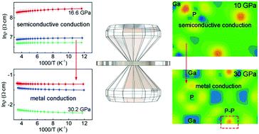
In situ impedance measurement, resistivity measurements and first-principles calculations have been performed to investigate the effect of high pressure (up to 30.2 GPa) on the metallization and dielectric properties of GaP. It is found that the carrier transport process changes from mixed grain and grain boundary conduction to pure grain conduction at 5.8 GPa, and due to pressure-induced structural phase transition, the resistance drops drastically by three orders of magnitude at 25.5 GPa. Temperature dependence of resistivity measurements and band structure calculations suggest the occurrence of a semiconductor–metal transition. Combining differential charge density and dielectric analysis, it is observed that the electron localization is weakened, which leads to increased polarization and larger relative permittivity in the zb structure. After the phase transition, both the polarization and the relative permittivity decrease. Pressure increases the complex dielectric constant and dielectric loss factor, due to the increase in relaxation polarization and the scattering effect of carriers. Moreover, by comparing the high-pressure behavior of GaP, GaAs and GaSb, the changes in the electronic structure and electric transport process caused by the phase transition can be understood, which can enable us to better understand the metallization behavior and dielectric properties of Ga-based III–V family semiconductors under pressure, and stimulate the design and modification of other related group III–V semiconductors for optoelectronic devices and sensors.
中文翻译:

压力对 GaP 金属化和介电性能的影响
就地已经进行了阻抗测量、电阻率测量和第一性原理计算,以研究高压(高达 30.2 GPa)对 GaP 的金属化和介电特性的影响。发现载流子传输过程在5.8 GPa时从混合晶粒和晶界传导转变为纯晶粒传导,并且由于压力诱导的结构相变,电阻在25.5 GPa时急剧下降三个数量级。电阻率测量和能带结构计算的温度依赖性表明发生了半导体-金属转变。结合微分电荷密度和介电分析,观察到电子局域化减弱,这导致 zb 结构中极化增加和更大的相对介电常数。在相变之后,极化和相对介电常数都降低。由于弛豫极化的增加和载流子的散射效应,压力会增加复介电常数和介电损耗因子。此外,通过比较 GaP、GaAs 和 GaSb 的高压行为,可以了解相变引起的电子结构和电输运过程的变化,这可以使我们更好地了解 Ga 的金属化行为和介电性能基于 III-V 族半导体的压力,并刺激用于光电器件和传感器的其他相关 III-V 族半导体的设计和修改。由于弛豫极化的增加和载流子的散射效应,压力会增加复介电常数和介电损耗因子。此外,通过比较 GaP、GaAs 和 GaSb 的高压行为,可以了解相变引起的电子结构和电输运过程的变化,这可以使我们更好地了解 Ga 的金属化行为和介电性能基于 III-V 族半导体的压力,并刺激用于光电器件和传感器的其他相关 III-V 族半导体的设计和修改。由于弛豫极化的增加和载流子的散射效应,压力会增加复介电常数和介电损耗因子。此外,通过比较 GaP、GaAs 和 GaSb 的高压行为,可以了解相变引起的电子结构和电输运过程的变化,这可以使我们更好地了解 Ga 的金属化行为和介电性能基于 III-V 族半导体的压力,并刺激用于光电器件和传感器的其他相关 III-V 族半导体的设计和修改。
更新日期:2021-11-24
中文翻译:
压力对 GaP 金属化和介电性能的影响
就地已经进行了阻抗测量、电阻率测量和第一性原理计算,以研究高压(高达 30.2 GPa)对 GaP 的金属化和介电特性的影响。发现载流子传输过程在5.8 GPa时从混合晶粒和晶界传导转变为纯晶粒传导,并且由于压力诱导的结构相变,电阻在25.5 GPa时急剧下降三个数量级。电阻率测量和能带结构计算的温度依赖性表明发生了半导体-金属转变。结合微分电荷密度和介电分析,观察到电子局域化减弱,这导致 zb 结构中极化增加和更大的相对介电常数。在相变之后,极化和相对介电常数都降低。由于弛豫极化的增加和载流子的散射效应,压力会增加复介电常数和介电损耗因子。此外,通过比较 GaP、GaAs 和 GaSb 的高压行为,可以了解相变引起的电子结构和电输运过程的变化,这可以使我们更好地了解 Ga 的金属化行为和介电性能基于 III-V 族半导体的压力,并刺激用于光电器件和传感器的其他相关 III-V 族半导体的设计和修改。由于弛豫极化的增加和载流子的散射效应,压力会增加复介电常数和介电损耗因子。此外,通过比较 GaP、GaAs 和 GaSb 的高压行为,可以了解相变引起的电子结构和电输运过程的变化,这可以使我们更好地了解 Ga 的金属化行为和介电性能基于 III-V 族半导体的压力,并刺激用于光电器件和传感器的其他相关 III-V 族半导体的设计和修改。由于弛豫极化的增加和载流子的散射效应,压力会增加复介电常数和介电损耗因子。此外,通过比较 GaP、GaAs 和 GaSb 的高压行为,可以了解相变引起的电子结构和电输运过程的变化,这可以使我们更好地了解 Ga 的金属化行为和介电性能基于 III-V 族半导体的压力,并刺激用于光电器件和传感器的其他相关 III-V 族半导体的设计和修改。


 京公网安备 11010802027423号