Our official English website, www.x-mol.net, welcomes your
feedback! (Note: you will need to create a separate account there.)
Atomically thin telluride multiheterostructures: toward spatial modulation of bandgaps
Nanoscale ( IF 5.8 ) Pub Date : 2021-10-29 , DOI: 10.1039/d1nr03746c Zheng Hao 1 , Kai Xu 1 , Junzhe Kang 1 , Changqiang Chen 2 , Wenjuan Zhu 1
Nanoscale ( IF 5.8 ) Pub Date : 2021-10-29 , DOI: 10.1039/d1nr03746c Zheng Hao 1 , Kai Xu 1 , Junzhe Kang 1 , Changqiang Chen 2 , Wenjuan Zhu 1
Affiliation
|
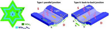
Lateral multiheterostructures with spatially modulated bandgaps have great potential for applications in high-performance electronic, optoelectronic and thermoelectric devices. Multiheterostructures based on transition metal tellurides are especially promising due to their tunable bandgap in a wide range and the rich variety of structural phases. However, the synthesis of telluride-based multiheterostructures remains a challenge due to the low activity of tellurium and the poor thermal stability of tellurium alloys. In this work, we synthesized monolayer WSe2−2xTe2x/WSe2−2yTe2y (x > y) multiheterostructures in situ using chemical vapor deposition (CVD). Photoluminescence analysis and Raman mapping confirm the spatial modulation of the bandgap in the radial direction. Furthermore, field-effect transistors with the channels parallel (type I) and perpendicular (type II) to the multiheterostructure rings were fabricated. Type I transistors exhibit enhanced ambipolar transport, due to the low energy bridges between the source and drain. Remarkably, the photocurrents in type I transistors are two orders of magnitude higher than those in type II transistors, which can be attributed to the fact that the photovoltaic photocurrents generated at the two heterojunctions are summed together in type I transistors, but they cancel each other in type II transistors. These multiheterostructures will provide a new platform for novel electronic/photonic devices with potential applications in broadband light sensing, highly sensitive imaging and ultrafast optoelectronic integrated circuits.
中文翻译:

原子级薄碲化物多异质结构:带隙的空间调制
具有空间调制带隙的横向多异质结构在高性能电子、光电和热电器件中具有巨大的应用潜力。基于过渡金属碲化物的多异质结构因其在宽范围内可调带隙和丰富多样的结构相而特别有前途。然而,由于碲的低活性和碲合金的热稳定性差,碲化物基多异质结构的合成仍然是一个挑战。在这项工作中,我们合成了单层WSE 2-2 X碲2 X / WSE 2-2 ý碲2 ý(X > Ý)multiheterostructures原位使用化学气相沉积 (CVD)。光致发光分析和拉曼映射证实了径向带隙的空间调制。此外,制造了通道平行(I 型)和垂直(II 型)多异质结构环的场效应晶体管。由于源极和漏极之间的低能量桥,I 型晶体管表现出增强的双极传输。值得注意的是,I型晶体管的光电流比II型晶体管高两个数量级,这可以归因于I型晶体管中两个异质结处产生的光伏光电流相加,但它们相互抵消在 II 型晶体管中。
更新日期:2021-11-23
中文翻译:
原子级薄碲化物多异质结构:带隙的空间调制
具有空间调制带隙的横向多异质结构在高性能电子、光电和热电器件中具有巨大的应用潜力。基于过渡金属碲化物的多异质结构因其在宽范围内可调带隙和丰富多样的结构相而特别有前途。然而,由于碲的低活性和碲合金的热稳定性差,碲化物基多异质结构的合成仍然是一个挑战。在这项工作中,我们合成了单层WSE 2-2 X碲2 X / WSE 2-2 ý碲2 ý(X > Ý)multiheterostructures原位使用化学气相沉积 (CVD)。光致发光分析和拉曼映射证实了径向带隙的空间调制。此外,制造了通道平行(I 型)和垂直(II 型)多异质结构环的场效应晶体管。由于源极和漏极之间的低能量桥,I 型晶体管表现出增强的双极传输。值得注意的是,I型晶体管的光电流比II型晶体管高两个数量级,这可以归因于I型晶体管中两个异质结处产生的光伏光电流相加,但它们相互抵消在 II 型晶体管中。


 京公网安备 11010802027423号