当前位置:
X-MOL 学术
›
Adv. Electron. Mater.
›
论文详情
Our official English website, www.x-mol.net, welcomes your
feedback! (Note: you will need to create a separate account there.)
On the Optoelectronic Mechanisms Ruling Ti-hyperdoped Si Photodiodes
Advanced Electronic Materials ( IF 5.3 ) Pub Date : 2021-11-16 , DOI: 10.1002/aelm.202100788 Eric García‐Hemme 1 , Daniel Caudevilla 1 , Sari Algaidy 1 , Francisco Pérez‐Zenteno 1 , Rodrigo García‐Hernansanz 1 , Javier Olea 1 , David Pastor 1 , Álvaro del Prado 1 , Enrique San Andrés 1 , Ignacio Mártil 1 , Germán González‐Díaz 1
Advanced Electronic Materials ( IF 5.3 ) Pub Date : 2021-11-16 , DOI: 10.1002/aelm.202100788 Eric García‐Hemme 1 , Daniel Caudevilla 1 , Sari Algaidy 1 , Francisco Pérez‐Zenteno 1 , Rodrigo García‐Hernansanz 1 , Javier Olea 1 , David Pastor 1 , Álvaro del Prado 1 , Enrique San Andrés 1 , Ignacio Mártil 1 , Germán González‐Díaz 1
Affiliation
|
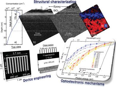
This work deepens the understanding of the optoelectronic mechanisms ruling hyperdoped-based photodevices and shows the potential of Ti hyperdoped-Si as a fully complementary metal-oxide semiconductor compatible material for room-temperature infrared photodetection technologies. By the combination of ion implantation and laser-based methods, ≈20 nm thin hyperdoped single-crystal Si layers with a Ti concentration as high as 1020 cm−3 are obtained. The Ti hyperdoped Si/p-Si photodiode shows a room temperature rectification factor at ±1 V of 509. Analysis of the temperature-dependent current–voltage characteristics shows that the transport is dominated by two mechanisms: a tunnel mechanism at low bias and a recombination process in the space charge region at high bias. A room-temperature sub-bandgap external quantum efficiency (EQE) extending to 2.5 µm wavelength is obtained. Temperature-dependent spectral photoresponse behavior reveals an increase of the EQE as the temperature decreases, showing a low-energy photoresponse edge at 0.45 eV and a high-energy photoresponse edge at 0.67 eV. Temperature behavior of the open-circuit voltage correlates with the high-energy photoresponse edge. A model is proposed to relate the optoelectronic mechanisms to sub-bandgap optical transitions involving an impurity band. This model is supported by numerical semiconductor device simulations using the SCAPS software.
中文翻译:

论支配钛超掺杂硅光电二极管的光电机制
这项工作加深了对基于超掺杂的光电器件的光电机制的理解,并展示了 Ti 超掺杂硅作为室温红外光电探测技术的完全互补金属氧化物半导体兼容材料的潜力。通过离子注入和基于激光的方法相结合,得到了 ≈20 nm 薄的超掺杂单晶硅层,Ti 浓度高达 10 20 cm -3获得。Ti 超掺杂 Si/p-Si 光电二极管在 509 的 ±1 V 处显示出室温整流因子。对温度相关的电流-电压特性的分析表明,传输受两种机制支配:低偏压下的隧道机制和高偏压下空间电荷区的复合过程。获得了扩展到 2.5 µm 波长的室温子带隙外部量子效率 (EQE)。与温度相关的光谱光响应行为揭示了 EQE 随着温度的降低而增加,在 0.45 eV 处显示出低能光响应边缘,在 0.67 eV 处显示出高能光响应边缘。开路电压的温度行为与高能光响应边缘相关。提出了一种将光电机制与涉及杂质带的子带隙光学跃迁联系起来的模型。该模型由使用 SCAPS 软件的数值半导体器件模拟支持。
更新日期:2021-11-16
中文翻译:
论支配钛超掺杂硅光电二极管的光电机制
这项工作加深了对基于超掺杂的光电器件的光电机制的理解,并展示了 Ti 超掺杂硅作为室温红外光电探测技术的完全互补金属氧化物半导体兼容材料的潜力。通过离子注入和基于激光的方法相结合,得到了 ≈20 nm 薄的超掺杂单晶硅层,Ti 浓度高达 10 20 cm -3获得。Ti 超掺杂 Si/p-Si 光电二极管在 509 的 ±1 V 处显示出室温整流因子。对温度相关的电流-电压特性的分析表明,传输受两种机制支配:低偏压下的隧道机制和高偏压下空间电荷区的复合过程。获得了扩展到 2.5 µm 波长的室温子带隙外部量子效率 (EQE)。与温度相关的光谱光响应行为揭示了 EQE 随着温度的降低而增加,在 0.45 eV 处显示出低能光响应边缘,在 0.67 eV 处显示出高能光响应边缘。开路电压的温度行为与高能光响应边缘相关。提出了一种将光电机制与涉及杂质带的子带隙光学跃迁联系起来的模型。该模型由使用 SCAPS 软件的数值半导体器件模拟支持。


 京公网安备 11010802027423号