Applied Surface Science ( IF 6.3 ) Pub Date : 2021-11-06 , DOI: 10.1016/j.apsusc.2021.151806 Hongyan Zhu 1, 2 , Zhiyuan Shi 1 , Chao Zhang 1, 2 , Boxiang Gao 1, 2 , Ji Chen 1 , JiaXin Ding 3 , Mingjiang Jin 4 , Tianru Wu 1 , Guanghui Yu 1, 2
|
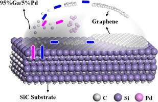
Direct growth of graphene on insulating substrate is highly desired for practical applications in two-dimensional electronics and optoelectronics. However, the controllable synthesis of large scale graphene films on dielectrics is still limited in thickness and crystallinity by the absence of catalyst. Here we develop a transfer-free method to synthesize continuous graphene films on various insulating substrates by using molten Ga-Pd alloy and silicon carbide (SiC) as catalyst and carbon source. The catalytic Ga-Pd alloy induces the decomposition of Si C bonds and promotes the formation of C-C sp2 at relatively low temperature around 1000 °C. The suitable carbon solubility of Ga-Pd alloy could also promote the fabrication of few-layer graphene films on the interface between alloy and SiC substrate as well as the upper surface of alloy. Furthermore, this strategy could be extended to the interfacial growth of graphene on other dielectrics by simply placing the substrate face down to the surface of molten alloy. The progress of this work may help to understand the mechanism of molten Ga-Pd alloy catalyzed interfacial growth of transfer-free graphene and benefit the application of graphene-based electronics and photonics in the future.
中文翻译:
熔融 Ga-Pd 合金催化石墨烯在介电基板上的界面生长
在二维电子学和光电子学的实际应用中,非常需要在绝缘基板上直接生长石墨烯。然而,由于缺乏催化剂,在电介质上可控合成大规模石墨烯薄膜的厚度和结晶度仍然受到限制。在这里,我们开发了一种无转移方法,通过使用熔融 Ga-Pd 合金和碳化硅 (SiC) 作为催化剂和碳源,在各种绝缘基板上合成连续的石墨烯薄膜。催化Ga-Pd合金诱导Si C键分解并促进CC sp 2的形成在 1000°C 左右的相对较低的温度下。Ga-Pd合金适当的碳溶解度也可以促进在合金和SiC衬底之间的界面以及合金上表面制备少层石墨烯薄膜。此外,这种策略可以扩展到石墨烯在其他电介质上的界面生长,只需将基板面朝下放置到熔融合金的表面即可。这项工作的进展可能有助于理解熔融 Ga-Pd 合金催化无转移石墨烯界面生长的机制,并有利于未来石墨烯电子学和光子学的应用。


 京公网安备 11010802027423号