当前位置:
X-MOL 学术
›
Adv. Electron. Mater.
›
论文详情
Our official English website, www.x-mol.net, welcomes your
feedback! (Note: you will need to create a separate account there.)
Crystal Phase Control during Epitaxial Hybridization of III-V Semiconductors with Silicon
Advanced Electronic Materials ( IF 5.3 ) Pub Date : 2021-10-25 , DOI: 10.1002/aelm.202100777 Marta Rio Calvo 1 , Jean‐Baptiste Rodriguez 1 , Charles Cornet 2 , Laurent Cerutti 1 , Michel Ramonda 3 , Achim Trampert 4 , Gilles Patriarche 5 , Éric Tournié 1
Advanced Electronic Materials ( IF 5.3 ) Pub Date : 2021-10-25 , DOI: 10.1002/aelm.202100777 Marta Rio Calvo 1 , Jean‐Baptiste Rodriguez 1 , Charles Cornet 2 , Laurent Cerutti 1 , Michel Ramonda 3 , Achim Trampert 4 , Gilles Patriarche 5 , Éric Tournié 1
Affiliation
|
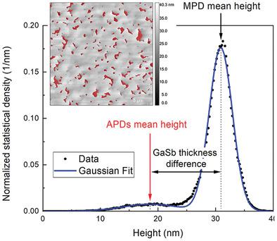
The formation and propagation of anti-phase boundaries (APBs) in the epitaxial growth of III-V semiconductors on Silicon is still the subject of great debate, despite the impressive number of studies focusing on this topic in the last past decades. The control of the layer phase is of major importance for the future realization of photonic integrated circuits that include efficient light sources or for new nano-electronic devices, for example. Here, it is experimentally demonstrated that the main-phase domain overgrows the anti-phase domains (APDs) because it grows faster. A large-scale analysis of the phase evolution based on reflection high-energy electron diffraction and atomic force microscopy in the case of the molecular beam epitaxy of GaSb on Silicon (001) substrate is presented. The growth rate difference between the two domains is accurately measured and is shown to come from the atomic step distribution at the III-V surface. The influence of the substrate preparation as well as of the growth condition on this distribution is also clarified.
中文翻译:

III-V 半导体与硅的外延杂化过程中的晶相控制
尽管在过去几十年中有大量研究关注这一主题,但在硅上的 III-V 半导体外延生长中反相边界 (APB) 的形成和传播仍然是备受争议的主题。例如,层相的控制对于包括高效光源的光子集成电路的未来实现或对于新的纳米电子器件具有重要意义。在这里,实验证明主相域长得比反相域(APDs)长,因为它生长得更快。提出了基于反射高能电子衍射和原子力显微镜的相变的大规模分析,在硅 (001) 衬底上的 GaSb 分子束外延的情况下。准确测量了两个域之间的生长速率差异,并显示出来自 III-V 表面的原子台阶分布。还阐明了基板制备以及生长条件对这种分布的影响。
更新日期:2021-10-25
中文翻译:
III-V 半导体与硅的外延杂化过程中的晶相控制
尽管在过去几十年中有大量研究关注这一主题,但在硅上的 III-V 半导体外延生长中反相边界 (APB) 的形成和传播仍然是备受争议的主题。例如,层相的控制对于包括高效光源的光子集成电路的未来实现或对于新的纳米电子器件具有重要意义。在这里,实验证明主相域长得比反相域(APDs)长,因为它生长得更快。提出了基于反射高能电子衍射和原子力显微镜的相变的大规模分析,在硅 (001) 衬底上的 GaSb 分子束外延的情况下。准确测量了两个域之间的生长速率差异,并显示出来自 III-V 表面的原子台阶分布。还阐明了基板制备以及生长条件对这种分布的影响。


 京公网安备 11010802027423号