当前位置:
X-MOL 学术
›
Phys. Rev. B
›
论文详情
Our official English website, www.x-mol.net, welcomes your
feedback! (Note: you will need to create a separate account there.)
Scanning ultrafast electron microscopy reveals photovoltage dynamics at a deeply buriedp−Si/SiO2interface
Physical Review B ( IF 3.2 ) Pub Date : 2021-10-26 , DOI: 10.1103/physrevb.104.l161303 S. R. Ellis 1 , N. C. Bartelt 1 , F. Léonard 1 , K. C. Celio 1 , E. J. Fuller 1 , D. R. Hughart 2 , D. Garland 2 , M. J. Marinella 2 , J. R. Michael 2 , D. W. Chandler 1 , B. Liao 3 , A. A. Talin 1
Physical Review B ( IF 3.2 ) Pub Date : 2021-10-26 , DOI: 10.1103/physrevb.104.l161303 S. R. Ellis 1 , N. C. Bartelt 1 , F. Léonard 1 , K. C. Celio 1 , E. J. Fuller 1 , D. R. Hughart 2 , D. Garland 2 , M. J. Marinella 2 , J. R. Michael 2 , D. W. Chandler 1 , B. Liao 3 , A. A. Talin 1
Affiliation
|
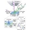
The understanding and control of charge carrier interactions with defects at buried insulator/semiconductor interfaces is essential for achieving optimum performance in modern electronics. Here, we report on the use of scanning ultrafast electron microscopy (SUEM) to remotely probe the dynamics of excited carriers at a Si surface buried below a thick thermal oxide. Our measurements illustrate a previously unidentified SUEM contrast mechanism, whereby optical modulation of the space-charge field in the semiconductor modulates the electric field in the thick oxide, thus affecting its secondary electron yield. By analyzing the SUEM contrast as a function of time and laser fluence we demonstrate the diffusion mediated capture of excited carriers by interfacial traps.
中文翻译:

扫描超快电子显微镜揭示了深埋 p-Si/SiO2 界面处的光电压动力学
了解和控制电荷载流子与掩埋绝缘体/半导体界面缺陷的相互作用对于实现现代电子产品的最佳性能至关重要。在这里,我们报告了使用扫描超快电子显微镜 (SUEM) 远程探测埋在厚热氧化物下方的 Si 表面上激发载流子的动力学。我们的测量结果说明了以前未知的 SUEM 对比机制,即半导体中空间电荷场的光学调制会调制厚氧化物中的电场,从而影响其二次电子产率。通过分析作为时间和激光能量密度函数的 SUEM 对比度,我们证明了界面陷阱对受激载流子的扩散介导捕获。
更新日期:2021-10-26
中文翻译:
扫描超快电子显微镜揭示了深埋 p-Si/SiO2 界面处的光电压动力学
了解和控制电荷载流子与掩埋绝缘体/半导体界面缺陷的相互作用对于实现现代电子产品的最佳性能至关重要。在这里,我们报告了使用扫描超快电子显微镜 (SUEM) 远程探测埋在厚热氧化物下方的 Si 表面上激发载流子的动力学。我们的测量结果说明了以前未知的 SUEM 对比机制,即半导体中空间电荷场的光学调制会调制厚氧化物中的电场,从而影响其二次电子产率。通过分析作为时间和激光能量密度函数的 SUEM 对比度,我们证明了界面陷阱对受激载流子的扩散介导捕获。


 京公网安备 11010802027423号