Our official English website, www.x-mol.net, welcomes your
feedback! (Note: you will need to create a separate account there.)
Multicolor Patterning of 2D Semiconductor Nanoplatelets
ACS Nano ( IF 15.8 ) Pub Date : 2021-10-19 , DOI: 10.1021/acsnano.1c05400 Mahdi Samadi Khoshkhoo 1 , Anatol Prudnikau 2 , Mohammad Reza Chashmejahanbin 1 , Ralf Helbig 3 , Vladimir Lesnyak 2 , Gianaurelio Cuniberti 1, 4
ACS Nano ( IF 15.8 ) Pub Date : 2021-10-19 , DOI: 10.1021/acsnano.1c05400 Mahdi Samadi Khoshkhoo 1 , Anatol Prudnikau 2 , Mohammad Reza Chashmejahanbin 1 , Ralf Helbig 3 , Vladimir Lesnyak 2 , Gianaurelio Cuniberti 1, 4
Affiliation
|
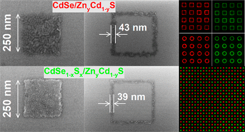
Nanocrystal micro/nanoarrays with multiplexed functionalities are of broad interest in the field of nanophotonics, cellular dynamics, and biosensing due to their tunable electrical and optical properties. This work focuses on the multicolor patterning of two-dimensional nanoplatelets (NPLs) via two sequential self-assembly and direct electron-beam lithography steps. By using scanning electron microscopy, atomic force microscopy, and fluorescence microscopy, we demonstrate the successful fabrication of fluorescent nanoarrays with a thickness of only two or three monolayers (7–11 nm) and a feature line width of ∼40 nm, which is three to four NPLs wide. To this end, first, large-area thin films of red-emitting CdSe/ZnyCd1–yS and green-emitting CdSe1–xSx/ZnyCd1–yS core/shell NPLs are fabricated based on Langmuir-type self-assembly at the liquid/air interface. By varying the concentration of ligands in the subphase, we investigate the effect of interaction potential on the film’s final characteristics to prepare thin superlattices suitable for the patterning step. Equipped with the ability to fabricate a uniform superlattice with a controlled thickness, we next perform nanopatterning on a thin film of NPLs utilizing a direct electron-beam lithography (EBL) technique. The effect of acceleration voltage, aperture size, and e-beam dosage on the nanopattern’s resolution and fidelity is investigated for both of the presented NPLs. After successfully optimizing EBL parameters to fabricate single-color nanopatterns, we finally focus on fabricating multicolor patterns. The obtained micro/nanoarrays provide us with an innovative experimental platform to investigate biological interactions as well as Förster resonance energy transfer.
中文翻译:

二维半导体纳米片的多色图案化
具有多重功能的纳米晶体微/纳米阵列由于其可调的电学和光学特性而在纳米光子学、细胞动力学和生物传感领域受到广泛关注。这项工作的重点是通过两个顺序自组装和直接电子束光刻步骤对二维纳米片 (NPL)进行多色图案化。通过使用扫描电子显微镜、原子力显微镜和荧光显微镜,我们证明了荧光纳米阵列的成功制造,其厚度仅为 2 或 3 个单层(7-11 nm),特征线宽度约为 40 nm,即 3到四个不良贷款宽。为此,首先,大面积的发红光 CdSe/Zn y Cd 1– y S 和发绿光CdSe 薄膜1– x S x /Zn y Cd 1– yS 核/壳 NPL 是基于液体/空气界面处的朗缪尔型自组装制造的。通过改变亚相中配体的浓度,我们研究了相互作用势对薄膜最终特性的影响,以制备适合图案化步骤的薄超晶格。具备制造具有受控厚度的均匀超晶格的能力,接下来我们利用直接电子束光刻 (EBL) 技术在 NPL 薄膜上进行纳米图案化。研究了加速电压、孔径大小和电子束剂量对纳米图案分辨率和保真度的影响,适用于两个提出的 NPL。在成功优化 EBL 参数以制造单色纳米图案后,我们最终专注于制造多色图案。
更新日期:2021-11-23
中文翻译:
二维半导体纳米片的多色图案化
具有多重功能的纳米晶体微/纳米阵列由于其可调的电学和光学特性而在纳米光子学、细胞动力学和生物传感领域受到广泛关注。这项工作的重点是通过两个顺序自组装和直接电子束光刻步骤对二维纳米片 (NPL)进行多色图案化。通过使用扫描电子显微镜、原子力显微镜和荧光显微镜,我们证明了荧光纳米阵列的成功制造,其厚度仅为 2 或 3 个单层(7-11 nm),特征线宽度约为 40 nm,即 3到四个不良贷款宽。为此,首先,大面积的发红光 CdSe/Zn y Cd 1– y S 和发绿光CdSe 薄膜1– x S x /Zn y Cd 1– yS 核/壳 NPL 是基于液体/空气界面处的朗缪尔型自组装制造的。通过改变亚相中配体的浓度,我们研究了相互作用势对薄膜最终特性的影响,以制备适合图案化步骤的薄超晶格。具备制造具有受控厚度的均匀超晶格的能力,接下来我们利用直接电子束光刻 (EBL) 技术在 NPL 薄膜上进行纳米图案化。研究了加速电压、孔径大小和电子束剂量对纳米图案分辨率和保真度的影响,适用于两个提出的 NPL。在成功优化 EBL 参数以制造单色纳米图案后,我们最终专注于制造多色图案。


 京公网安备 11010802027423号