当前位置:
X-MOL 学术
›
Adv. Electron. Mater.
›
论文详情
Our official English website, www.x-mol.net, welcomes your
feedback! (Note: you will need to create a separate account there.)
Charge Transfer at the Hetero-Interface of WSe2/InSe Induces Efficient Doping to Achieve Multi-Functional Lateral Homo-Junctions
Advanced Electronic Materials ( IF 5.3 ) Pub Date : 2021-10-15 , DOI: 10.1002/aelm.202100584 Bo Xu 1 , Yang Li 1, 2 , Zhao‐Yuan Sun 3 , Ze Zhao 1 , Li Yang 1 , Feng Gao 2 , Ping‐An Hu 1, 2 , Liang Zhen 1, 2, 4 , Cheng‐Yan Xu 2, 4
Advanced Electronic Materials ( IF 5.3 ) Pub Date : 2021-10-15 , DOI: 10.1002/aelm.202100584 Bo Xu 1 , Yang Li 1, 2 , Zhao‐Yuan Sun 3 , Ze Zhao 1 , Li Yang 1 , Feng Gao 2 , Ping‐An Hu 1, 2 , Liang Zhen 1, 2, 4 , Cheng‐Yan Xu 2, 4
Affiliation
|
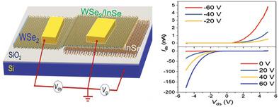
Charge transfer at the hetero-interface is at the center of van der Waals (vdWs) heterostructure devices for multi-functional applications. Compared with the extensively investigated photogenerated carrier transfer driven by the built-in electric field from the conduction or valence band offset, the charge transfer due to the Fermi level difference of the two adjacent constitutes, and its influence on the opto-/electronic performance of vdWs heterostructure devices are not clarified. Herein, by taking an example of WSe2/InSe heterostructure, it is demonstrated that the charge transfer at the hetero-interface is an efficient “doping” strategy to dramatically modulate the carrier densities of atomically thin counterparts due to the extension of “band bending” across the entire heterostructure, paving the way for the creation of lateral WSe2 p-n and n-n+ homo-junctions with multi-functionalities, including promising rectification, photovoltaic, and photodetection abilities. Moreover, the device physics of lateral homo-junctions, including potential distribution, band diagram, and photocurrent generation mechanisms, is revealed by gate-dependent Kelvin probe force microscopy and scanning photocurrent measurements. This work not only provides a general avenue to build 2D lateral homo-junctions, but also give deeper insights into the device physics of the junctions by coupling scanning probe and scanning photocurrent techniques.
中文翻译:

WSe2/InSe 异质界面的电荷转移诱导有效掺杂以实现多功能横向同质结
异质界面的电荷转移是多功能应用的范德华 (vdWs) 异质结构器件的中心。与广泛研究的由导带或价带偏移的内置电场驱动的光生载流子转移相比,由于两个相邻结构的费米能级差引起的电荷转移及其对光电性能的影响vdWs 异质结构器件没有明确。这里以WSe 2为例/InSe异质结构,证明异质界面处的电荷转移是一种有效的“掺杂”策略,由于整个异质结构的“能带弯曲”延伸,从而显着调节原子级薄对应物的载流子密度,铺平了道路用于创建横向 WSe 2 pn 和 nn +具有多功能的同质结,包括有前途的整流、光伏和光电检测能力。此外,横向同质结的器件物理特性,包括电位分布、能带图和光电流产生机制,通过依赖于栅极的开尔文探针力显微镜和扫描光电流测量来揭示。这项工作不仅提供了构建 2D 横向同质结的通用途径,而且还通过耦合扫描探针和扫描光电流技术更深入地了解结的器件物理。
更新日期:2021-12-09
中文翻译:
WSe2/InSe 异质界面的电荷转移诱导有效掺杂以实现多功能横向同质结
异质界面的电荷转移是多功能应用的范德华 (vdWs) 异质结构器件的中心。与广泛研究的由导带或价带偏移的内置电场驱动的光生载流子转移相比,由于两个相邻结构的费米能级差引起的电荷转移及其对光电性能的影响vdWs 异质结构器件没有明确。这里以WSe 2为例/InSe异质结构,证明异质界面处的电荷转移是一种有效的“掺杂”策略,由于整个异质结构的“能带弯曲”延伸,从而显着调节原子级薄对应物的载流子密度,铺平了道路用于创建横向 WSe 2 pn 和 nn +具有多功能的同质结,包括有前途的整流、光伏和光电检测能力。此外,横向同质结的器件物理特性,包括电位分布、能带图和光电流产生机制,通过依赖于栅极的开尔文探针力显微镜和扫描光电流测量来揭示。这项工作不仅提供了构建 2D 横向同质结的通用途径,而且还通过耦合扫描探针和扫描光电流技术更深入地了解结的器件物理。


 京公网安备 11010802027423号