Our official English website, www.x-mol.net, welcomes your
feedback! (Note: you will need to create a separate account there.)
Visualizing Band Profiles of Gate-Tunable Junctions in MoS2/WSe2 Heterostructure Transistors
ACS Nano ( IF 15.8 ) Pub Date : 2021-10-15 , DOI: 10.1021/acsnano.1c05491 Xinzuo Sun 1, 2 , Yan Chen 3 , Zhiwei Li 4 , Yu Han 1 , Qin Zhou 1 , Binbin Wang 1 , Takashi Taniguchi 5 , Kenji Watanabe 6 , Aidi Zhao 1 , Jianlu Wang 3 , Yuan Liu 4 , Jiamin Xue 1
ACS Nano ( IF 15.8 ) Pub Date : 2021-10-15 , DOI: 10.1021/acsnano.1c05491 Xinzuo Sun 1, 2 , Yan Chen 3 , Zhiwei Li 4 , Yu Han 1 , Qin Zhou 1 , Binbin Wang 1 , Takashi Taniguchi 5 , Kenji Watanabe 6 , Aidi Zhao 1 , Jianlu Wang 3 , Yuan Liu 4 , Jiamin Xue 1
Affiliation
|
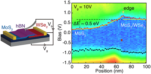
Heterostructure devices based on two-dimensional materials have been under intensive study due to their intriguing electrical and optical properties. One key factor in understanding these devices is their nanometer-scale band profiles, which is challenging to obtain in devices. Here, we use a technique named contact-mode scanning tunneling spectroscopy to directly visualize the band profiles of MoS2/WSe2 heterostructure devices at different gate voltages with nanometer resolution. The long-held view of a conventional p–n junction in the MoS2/WSe2 heterostructure is reexamined. Due to strong inter- and intralayer charge transfer, the MoS2 layer in contact with WSe2 is found to convert from n-type to p-type, and a series of gate-tunable p–n and p–p+ junctions are developed in the devices. Highly conductive edges are also discovered which could strongly affect the device properties.
中文翻译:

可视化 MoS2/WSe2 异质结构晶体管中栅极可调结的能带分布
基于二维材料的异质结构器件由于其有趣的电学和光学特性而受到深入研究。理解这些设备的一个关键因素是它们的纳米级能带分布,这在设备中很难获得。在这里,我们使用一种称为接触模式扫描隧道光谱的技术,以纳米分辨率直接可视化不同栅极电压下的 MoS 2 /WSe 2异质结构器件的能带分布。重新审视长期以来对 MoS 2 /WSe 2异质结构中传统 p-n 结的看法。由于强烈的层间和层内电荷转移,与 WSe 2接触的 MoS 2层发现从 n 型转换为 p 型,并且在器件中开发了一系列栅极可调 p-n 和 p-p +结。还发现了可能强烈影响器件性能的高导电边缘。
更新日期:2021-10-26
中文翻译:
可视化 MoS2/WSe2 异质结构晶体管中栅极可调结的能带分布
基于二维材料的异质结构器件由于其有趣的电学和光学特性而受到深入研究。理解这些设备的一个关键因素是它们的纳米级能带分布,这在设备中很难获得。在这里,我们使用一种称为接触模式扫描隧道光谱的技术,以纳米分辨率直接可视化不同栅极电压下的 MoS 2 /WSe 2异质结构器件的能带分布。重新审视长期以来对 MoS 2 /WSe 2异质结构中传统 p-n 结的看法。由于强烈的层间和层内电荷转移,与 WSe 2接触的 MoS 2层发现从 n 型转换为 p 型,并且在器件中开发了一系列栅极可调 p-n 和 p-p +结。还发现了可能强烈影响器件性能的高导电边缘。


 京公网安备 11010802027423号