Our official English website, www.x-mol.net, welcomes your feedback! (Note: you will need to create a separate account there.)
Experimental Realization and Phase Engineering of a Two-Dimensional SnSb Binary Honeycomb Lattice
ACS Nano ( IF 17.1 ) Pub Date : 2021-10-14 , DOI: 10.1021/acsnano.1c05583 Heping Li 1 , Dechun Zhou 2 , Qingyuan He 3 , Nan Si 2, 3 , Benwu Xin 3 , Saiyu Bu 3 , Qingmin Ji 2 , Hui Li 1 , Harald Fuchs 2, 4, 5 , Tianchao Niu 2
ACS Nano ( IF 17.1 ) Pub Date : 2021-10-14 , DOI: 10.1021/acsnano.1c05583 Heping Li 1 , Dechun Zhou 2 , Qingyuan He 3 , Nan Si 2, 3 , Benwu Xin 3 , Saiyu Bu 3 , Qingmin Ji 2 , Hui Li 1 , Harald Fuchs 2, 4, 5 , Tianchao Niu 2
Affiliation
|
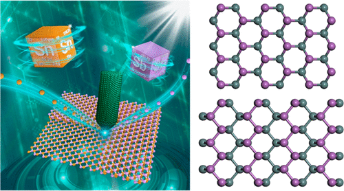
Binary two-dimensional (2D) materials comprising main group elements with several phases of AB and AB2 stoichiometry provide significantly rich physics and application potentials. We present the epitaxial growth of two phases of atomically thin SnSb on a Cu2Sb surface alloy under ultrahigh-vacuum (UHV) conditions. Theoretical studies predict that these 2D SnSb sheets adopt the atomic configurations similar to those of black and blue phosphorene but with Sb–Sn–Sn–Sb motif (R- and H-phases) holding an indirect band gap of 0.20 and 0.85 eV, respectively. Our low-temperature (77 K) scanning tunneling microscopy characterizations, and first-principles theoretical calculations, reveal the atomic structures and semiconducting properties of the most stable H-phase, displaying a commensurate lattice growth mode on Cu2Sb(111) but a weak interfacial interaction. Strain-engineered band gap, effective mass, and Young’s Modulus of the most stable H-phase are further explored theoretically. These results suggest that 2D SnSb with intriguing properties has great potential for electronics in an atomically thin platform.
中文翻译:

二维SnSb二元蜂窝晶格的实验实现和相位工程
包含具有AB和AB 2化学计量学数相的主族元素的二元二维(2D)材料提供了非常丰富的物理和应用潜力。我们展示了两相原子级薄 SnSb 在 Cu 2上的外延生长超高真空 (UHV) 条件下的 Sb 表面合金。理论研究预测,这些 2D SnSb 片采用类似于黑色和蓝色磷烯的原子构型,但 Sb-Sn-Sn-Sb 基序(R 相和 H 相)的间接带隙分别为 0.20 和 0.85 eV . 我们的低温 (77 K) 扫描隧道显微镜表征和第一性原理理论计算揭示了最稳定的 H 相的原子结构和半导体特性,在 Cu 2上显示出相应的晶格生长模式Sb(111) 但界面相互作用较弱。从理论上进一步探讨了最稳定 H 相的应变工程带隙、有效质量和杨氏模量。这些结果表明,具有有趣特性的 2D SnSb 在原子级薄平台中具有巨大的电子学潜力。
更新日期:2021-10-26
中文翻译:
二维SnSb二元蜂窝晶格的实验实现和相位工程
包含具有AB和AB 2化学计量学数相的主族元素的二元二维(2D)材料提供了非常丰富的物理和应用潜力。我们展示了两相原子级薄 SnSb 在 Cu 2上的外延生长超高真空 (UHV) 条件下的 Sb 表面合金。理论研究预测,这些 2D SnSb 片采用类似于黑色和蓝色磷烯的原子构型,但 Sb-Sn-Sn-Sb 基序(R 相和 H 相)的间接带隙分别为 0.20 和 0.85 eV . 我们的低温 (77 K) 扫描隧道显微镜表征和第一性原理理论计算揭示了最稳定的 H 相的原子结构和半导体特性,在 Cu 2上显示出相应的晶格生长模式Sb(111) 但界面相互作用较弱。从理论上进一步探讨了最稳定 H 相的应变工程带隙、有效质量和杨氏模量。这些结果表明,具有有趣特性的 2D SnSb 在原子级薄平台中具有巨大的电子学潜力。


 京公网安备 11010802027423号