当前位置:
X-MOL 学术
›
Acc. Chem. Res.
›
论文详情
Our official English website, www.x-mol.net, welcomes your
feedback! (Note: you will need to create a separate account there.)
Colloidal Two-Dimensional Metal Chalcogenides: Realization and Application of the Structural Anisotropy
Accounts of Chemical Research ( IF 16.4 ) Pub Date : 2021-10-08 , DOI: 10.1021/acs.accounts.1c00209 Ziyi Hu 1, 2 , Ryan O'Neill 1 , Rostyslav Lesyuk 3, 4, 5 , Christian Klinke 1, 3, 6
Accounts of Chemical Research ( IF 16.4 ) Pub Date : 2021-10-08 , DOI: 10.1021/acs.accounts.1c00209 Ziyi Hu 1, 2 , Ryan O'Neill 1 , Rostyslav Lesyuk 3, 4, 5 , Christian Klinke 1, 3, 6
Affiliation
|
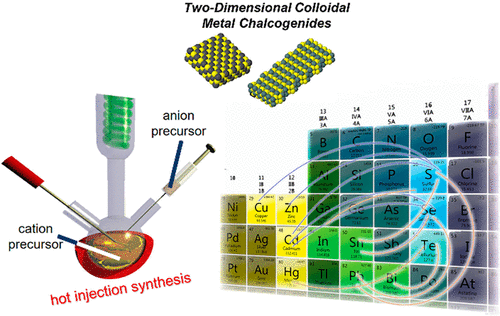
Due to the spatial confinement, two-dimensional metal chalcogenides display an extraordinary optical response and carrier transport ability. Solution-based synthesis techniques such as colloidal hot injection and ion exchange provide a cost-effective way to fabricate such low-dimensional semiconducting nanocrystals. Over the years, developments in colloidal chemistry made it possible to synthesize various kinds of ultrathin colloidal nanoplatelets, including wurtzite- and zinc blende-type CdSe, rock salt PbS, black phosphorus-like SnX (X = S or Se), hexagonal copper sulfides, selenides, and even transition metal dichalcogenides like MoS2. By altering experimental conditions and applying capping ligands with specific functional groups, it is possible to accurately tune the dimensionality, geometry, and consequently the optical properties of these colloidal metal chalcogenide crystals. Here, we review recent progress in the syntheses of two-dimensional colloidal metal chalcogenides (CMCs) and property characterizations based on optical spectroscopy or device-related measurements. The discoveries shine a light on their huge prospect for applications in areas such as photovoltaics, optoelectronics, and spintronics. In specific, the formation mechanisms of two-dimensional CMCs are discussed. The growth of colloidal nanocrystals into a two-dimensional shape is found to require either an intrinsic structural asymmetry or the assist of coexisted ligand molecules, which act as lamellar double-layer templates or “facet” the crystals via selective adsorption. By performing optical characterizations and especially ultrafast spectroscopic measurements on these two-dimensional CMCs, their unique electronic and excitonic features are revealed. A strong dependence of optical transition energies linked to both interband and inter-subband processes on the crystal geometry can be verified, highlighting a tremendous confinement effect in such nanocrystals. With the self-assembly of two-dimensional nanocrystals or coupling of different phases by growing heterostructures, unconventional optical performances such as charge transfer state generation or efficient Förster resonance energy transfer are discovered. The growth of large-scale individualized PbS and SnS nanosheets can be realized by facile hot injection techniques, which gives the opportunity to investigate the charge carrier behavior within a single nanocrystal. According to the results of the device-based measurements on these individualized crystals, structure asymmetry-induced anisotropic electrical responses and Rashba effects caused by a splitting of spin-resolved bands in the momentum space due to strong spin–orbit-coupling are demonstrated. It is foreseen that such geometry-controlled, large-scale two-dimensional CMCs can be the ideal materials used for designing high-efficiency photonics and electronics.
中文翻译:

胶体二维金属硫属化物:结构各向异性的实现与应用
由于空间限制,二维金属硫属化物显示出非凡的光学响应和载流子传输能力。基于溶液的合成技术,如胶体热注射和离子交换,为制造这种低维半导体纳米晶体提供了一种经济有效的方法。多年来,胶体化学的发展使得合成各种超薄胶体纳米片成为可能,包括纤锌矿型和闪锌矿型 CdSe、岩盐 PbS、类黑磷 SnX(X = S 或 Se)、六方硫化铜、硒化物,甚至过渡金属二硫属化物,如 MoS 2. 通过改变实验条件和应用具有特定官能团的封端配体,可以准确地调整这些胶体金属硫属化物晶体的尺寸、几何形状以及光学特性。在这里,我们回顾了二维胶体金属硫属元素化物 (CMC) 的合成和基于光谱或设备相关测量的特性表征的最新进展。这些发现揭示了它们在光伏、光电子和自旋电子学等领域的巨大应用前景。具体讨论了二维CMCs的形成机制。发现胶体纳米晶体生长成二维形状需要固有的结构不对称性或共存配体分子的帮助,通过选择性吸附充当层状双层模板或“刻面”晶体。通过对这些二维 CMC 进行光学表征,尤其是超快光谱测量,揭示了它们独特的电子和激子特征。可以验证与带间和子带间过程相关的光学跃迁能量对晶体几何形状的强烈依赖性,突出了这种纳米晶体中的巨大限制效应。通过二维纳米晶体的自组装或通过生长异质结构耦合不同相,发现了非常规的光学性能,例如电荷转移状态的产生或有效的 Förster 共振能量转移。可以通过简便的热注入技术实现大规模个体化 PbS 和 SnS 纳米片的生长,这为研究单个纳米晶体内的电荷载流子行为提供了机会。根据对这些个体化晶体的基于设备的测量结果,证明了结构不对称引起的各向异性电响应和 Rashba 效应,这是由于强自旋轨道耦合导致动量空间中自旋分辨带分裂引起的。可以预见,这种几何控制的大规模二维 CMC 可以成为用于设计高效光子学和电子学的理想材料。根据对这些个体化晶体的基于设备的测量结果,证明了结构不对称引起的各向异性电响应和 Rashba 效应,这是由于强自旋轨道耦合导致动量空间中自旋分辨带分裂引起的。可以预见,这种几何控制的大规模二维 CMC 可以成为用于设计高效光子学和电子学的理想材料。根据对这些个体化晶体的基于设备的测量结果,证明了结构不对称引起的各向异性电响应和由强自旋轨道耦合引起的动量空间中自旋分辨带分裂引起的 Rashba 效应。可以预见,这种几何控制的大规模二维 CMC 可以成为用于设计高效光子学和电子学的理想材料。
更新日期:2021-10-19
中文翻译:
胶体二维金属硫属化物:结构各向异性的实现与应用
由于空间限制,二维金属硫属化物显示出非凡的光学响应和载流子传输能力。基于溶液的合成技术,如胶体热注射和离子交换,为制造这种低维半导体纳米晶体提供了一种经济有效的方法。多年来,胶体化学的发展使得合成各种超薄胶体纳米片成为可能,包括纤锌矿型和闪锌矿型 CdSe、岩盐 PbS、类黑磷 SnX(X = S 或 Se)、六方硫化铜、硒化物,甚至过渡金属二硫属化物,如 MoS 2. 通过改变实验条件和应用具有特定官能团的封端配体,可以准确地调整这些胶体金属硫属化物晶体的尺寸、几何形状以及光学特性。在这里,我们回顾了二维胶体金属硫属元素化物 (CMC) 的合成和基于光谱或设备相关测量的特性表征的最新进展。这些发现揭示了它们在光伏、光电子和自旋电子学等领域的巨大应用前景。具体讨论了二维CMCs的形成机制。发现胶体纳米晶体生长成二维形状需要固有的结构不对称性或共存配体分子的帮助,通过选择性吸附充当层状双层模板或“刻面”晶体。通过对这些二维 CMC 进行光学表征,尤其是超快光谱测量,揭示了它们独特的电子和激子特征。可以验证与带间和子带间过程相关的光学跃迁能量对晶体几何形状的强烈依赖性,突出了这种纳米晶体中的巨大限制效应。通过二维纳米晶体的自组装或通过生长异质结构耦合不同相,发现了非常规的光学性能,例如电荷转移状态的产生或有效的 Förster 共振能量转移。可以通过简便的热注入技术实现大规模个体化 PbS 和 SnS 纳米片的生长,这为研究单个纳米晶体内的电荷载流子行为提供了机会。根据对这些个体化晶体的基于设备的测量结果,证明了结构不对称引起的各向异性电响应和 Rashba 效应,这是由于强自旋轨道耦合导致动量空间中自旋分辨带分裂引起的。可以预见,这种几何控制的大规模二维 CMC 可以成为用于设计高效光子学和电子学的理想材料。根据对这些个体化晶体的基于设备的测量结果,证明了结构不对称引起的各向异性电响应和 Rashba 效应,这是由于强自旋轨道耦合导致动量空间中自旋分辨带分裂引起的。可以预见,这种几何控制的大规模二维 CMC 可以成为用于设计高效光子学和电子学的理想材料。根据对这些个体化晶体的基于设备的测量结果,证明了结构不对称引起的各向异性电响应和由强自旋轨道耦合引起的动量空间中自旋分辨带分裂引起的 Rashba 效应。可以预见,这种几何控制的大规模二维 CMC 可以成为用于设计高效光子学和电子学的理想材料。


 京公网安备 11010802027423号