当前位置:
X-MOL 学术
›
ACS Photonics
›
论文详情
Our official English website, www.x-mol.net, welcomes your
feedback! (Note: you will need to create a separate account there.)
Heterostructured Vertical Organic Transistor for High-Performance Optoelectronic Memory and Artificial Synapse
ACS Photonics ( IF 6.5 ) Pub Date : 2021-10-06 , DOI: 10.1021/acsphotonics.1c01167 Chuangsong Gao 1, 2 , Huihuang Yang 1, 2 , Enlong Li 1, 2 , Yujie Yan 1, 2 , Lihua He 1, 2 , Huipeng Chen 1, 2 , Zhixian Lin 1, 3 , Tailiang Guo 1, 2
ACS Photonics ( IF 6.5 ) Pub Date : 2021-10-06 , DOI: 10.1021/acsphotonics.1c01167 Chuangsong Gao 1, 2 , Huihuang Yang 1, 2 , Enlong Li 1, 2 , Yujie Yan 1, 2 , Lihua He 1, 2 , Huipeng Chen 1, 2 , Zhixian Lin 1, 3 , Tailiang Guo 1, 2
Affiliation
|
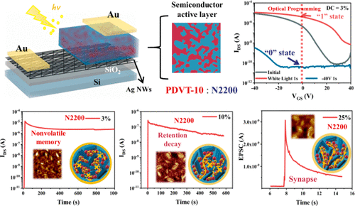
Organic field-effect transistor (OFET) memory has received widespread attention due to its easy integration, precise charge modulation, and multi-level memory. However, the performance of organic memory still needs to be improved for its practical application, and the reported technologies are strongly dependent on an additional charge-trapping layer, which increases the complexity of the device. Here, we report a heterostructured vertical organic memory transistor, which uses a p/n semiconductor bulk heterojunction as a semiconductor layer without using any additional charge-trapping layers. The device exhibits a large memory window of 52 V, and the memory ratio reaches 105 through electrical operation. Benefiting from the formation of the p/n semiconductor interface and the nanometer-scale transmission length, under the stimulation of visible light, the device achieved a 58 V memory window, high memory ratio 105, and retention characteristics of over 10 years, which is better than those of most reported optical organic memory devices. More interestingly, we found that as the level of the doping in the n-type semiconductor increased, the device could transform from nonvolatile memory to artificial synapse, which is associated with the morphology of a heterojunction structure. Hence, we demonstrate a novel technique to manufacture high-performance nonvolatile optoelectronic memory and artificial synapse, which shows great potential in OFET-based memory and neuromorphic devices.
中文翻译:

用于高性能光电存储器和人工突触的异质结构垂直有机晶体管
有机场效应晶体管(OFET)存储器因其易于集成、精确的电荷调制和多级存储器而受到广泛关注。然而,有机存储器的性能在实际应用中仍有待提高,而且报道的技术强烈依赖于额外的电荷俘获层,这增加了器件的复杂性。在这里,我们报告了一种异质结构垂直有机存储晶体管,它使用 p/n 半导体体异质结作为半导体层,而不使用任何额外的电荷俘获层。该器件具有52 V的大内存窗口,内存比达到10 5通过电动操作。得益于p/n半导体界面的形成和纳米级的传输长度,在可见光的刺激下,该器件实现了58V的存储窗口、10 5 的高存储比和10年以上的保持特性,优于大多数报道的光学有机存储器件。更有趣的是,我们发现随着 n 型半导体中掺杂水平的增加,器件可以从非易失性存储器转变为人工突触,这与异质结结构的形态有关。因此,我们展示了一种制造高性能非易失性光电存储器和人工突触的新技术,该技术在基于 OFET 的存储器和神经形态器件中显示出巨大的潜力。
更新日期:2021-10-20
中文翻译:
用于高性能光电存储器和人工突触的异质结构垂直有机晶体管
有机场效应晶体管(OFET)存储器因其易于集成、精确的电荷调制和多级存储器而受到广泛关注。然而,有机存储器的性能在实际应用中仍有待提高,而且报道的技术强烈依赖于额外的电荷俘获层,这增加了器件的复杂性。在这里,我们报告了一种异质结构垂直有机存储晶体管,它使用 p/n 半导体体异质结作为半导体层,而不使用任何额外的电荷俘获层。该器件具有52 V的大内存窗口,内存比达到10 5通过电动操作。得益于p/n半导体界面的形成和纳米级的传输长度,在可见光的刺激下,该器件实现了58V的存储窗口、10 5 的高存储比和10年以上的保持特性,优于大多数报道的光学有机存储器件。更有趣的是,我们发现随着 n 型半导体中掺杂水平的增加,器件可以从非易失性存储器转变为人工突触,这与异质结结构的形态有关。因此,我们展示了一种制造高性能非易失性光电存储器和人工突触的新技术,该技术在基于 OFET 的存储器和神经形态器件中显示出巨大的潜力。


 京公网安备 11010802027423号