当前位置:
X-MOL 学术
›
Phys. Rev. B
›
论文详情
Our official English website, www.x-mol.net, welcomes your
feedback! (Note: you will need to create a separate account there.)
Ni3+-induced semiconductor-to-metal transition in spinel nickel cobaltite thin films
Physical Review B ( IF 3.2 ) Pub Date : 2021-09-23 , DOI: 10.1103/physrevb.104.125136 X. C. Huang 1 , W.-W. Li 2 , S. Zhang 3 , F. E. Oropeza 4 , G. Gorni 5 , V. A. de la Peña-O’Shea 4 , T.-L. Lee 6 , M. Wu 7 , L.-S. Wang 8 , D.-C. Qi 9 , L. Qiao 3 , J. Cheng 1 , K. H. L. Zhang 1
Physical Review B ( IF 3.2 ) Pub Date : 2021-09-23 , DOI: 10.1103/physrevb.104.125136 X. C. Huang 1 , W.-W. Li 2 , S. Zhang 3 , F. E. Oropeza 4 , G. Gorni 5 , V. A. de la Peña-O’Shea 4 , T.-L. Lee 6 , M. Wu 7 , L.-S. Wang 8 , D.-C. Qi 9 , L. Qiao 3 , J. Cheng 1 , K. H. L. Zhang 1
Affiliation
|
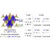
In this paper, we report insights into the local atomic and electronic structure of epitaxial thin films and its correlation with electrical, optical, and magnetic properties. We grew structurally well-defined epitaxial thin films with controlled properties on substrates using pulsed laser deposition. Films grown at low temperatures () exhibit a ferrimagnetic and metallic behavior, while those grown at high temperatures are nonmagnetic semiconductors. The electronic structure and cation local atomic coordination of the respective films were investigated using a combination of resonant photoemission spectroscopy, x-ray absorption spectroscopy, and ab initio calculations. Our results unambiguously reveal that the valence state promoted at low growth temperature introduces delocalized -derived states at the Fermi level (), responsible for the metallic state in , while the -related state is more localized at higher binding energy. In the semiconducting films, the valence state of Ni is lowered and . Further structural and defect chemistry studies indicate that the formation of oxygen vacancies and secondary CoO phases at high growth temperature are responsible for the valence state in . The -related state becomes localized away from , opening a band gap for a semiconducting state. The band gap of the semiconducting is estimated to be , which is much smaller than the quoted values in the literature ranging from 1.1 to 2.58 eV. Despite the small band gap, its optical transition is dipole forbidden, and therefore, the semiconducting still shows reasonable transparency in the infrared-visible light region. The present insights into the role of in determining the electronic structure and defect chemistry of provide important guidance for use of in electrocatalysis and opto-electronics.
中文翻译:

Ni3+ 诱导尖晶石镍钴酸盐薄膜中的半导体-金属转变
在本文中,我们报告了对局部原子和电子结构的见解 外延薄膜及其与电、光和磁特性的相关性。我们在结构上发展明确 具有可控特性的外延薄膜 使用脉冲激光沉积的基板。在低温下生长的薄膜() 表现出亚铁磁性和金属行为,而那些在高温下生长的是非磁性半导体。使用共振光电发射光谱、X 射线吸收光谱和ab initio计算的组合研究了各个薄膜的电子结构和阳离子局部原子配位。我们的结果明确表明, 在低生长温度下促进的价态引入离域 - 费米能级的派生态 (),负责金属状态 ,而 -相关状态更集中于更高的结合能。在半导体薄膜中,Ni 的价态降低,. 进一步的结构和缺陷化学研究表明,在高生长温度下形成氧空位和二次 CoO 相是导致 价态在 . 这-相关状态变得本地化远离 ,为半导体状态打开带隙。半导体带隙 估计是 ,这远小于文献中引用的值,范围从 1.1 到 2.58 eV。尽管带隙很小,但它的光学跃迁是 偶极子被禁止,因此,半导体 在红外可见光区域仍显示出合理的透明度。目前对角色的见解 在确定电子结构和缺陷化学 提供重要的使用指导 在电催化和光电子领域。
更新日期:2021-09-24
中文翻译:
Ni3+ 诱导尖晶石镍钴酸盐薄膜中的半导体-金属转变
在本文中,我们报告了对局部原子和电子结构的见解 外延薄膜及其与电、光和磁特性的相关性。我们在结构上发展明确 具有可控特性的外延薄膜 使用脉冲激光沉积的基板。在低温下生长的薄膜() 表现出亚铁磁性和金属行为,而那些在高温下生长的是非磁性半导体。使用共振光电发射光谱、X 射线吸收光谱和ab initio计算的组合研究了各个薄膜的电子结构和阳离子局部原子配位。我们的结果明确表明, 在低生长温度下促进的价态引入离域 - 费米能级的派生态 (),负责金属状态 ,而 -相关状态更集中于更高的结合能。在半导体薄膜中,Ni 的价态降低,. 进一步的结构和缺陷化学研究表明,在高生长温度下形成氧空位和二次 CoO 相是导致 价态在 . 这-相关状态变得本地化远离 ,为半导体状态打开带隙。半导体带隙 估计是 ,这远小于文献中引用的值,范围从 1.1 到 2.58 eV。尽管带隙很小,但它的光学跃迁是 偶极子被禁止,因此,半导体 在红外可见光区域仍显示出合理的透明度。目前对角色的见解 在确定电子结构和缺陷化学 提供重要的使用指导 在电催化和光电子领域。


 京公网安备 11010802027423号